Method for preparing vacuum zone melting high resistant silicon single crystal

A vacuum zone, high-resistance silicon technology, applied in the self-zone melting method, single crystal growth, single crystal growth and other directions, can solve the problems of high cross-sectional uniformity, high "minority carrier lifetime, and inability to produce ultra-high purity. Achieve the effect of increasing resistivity, improving device performance and stability

Active Publication Date: 2009-09-09
峨嵋半导体材料研究所
View PDF1 Cites 27 Cited by
  • Summary
  • Abstract
  • Description
  • Claims
  • Application Information

AI Technical Summary

Problems solved by technology

[0004] The purpose of the present invention is to provide a silicon single crystal that can produce such a silicon sing

Method used


Image

  • Method for preparing vacuum zone melting high resistant silicon single crystal
  • Method for preparing vacuum zone melting high resistant silicon single crystal

Examples


Embodiment 1

[0036] Example 1 Preparation method of vacuum zone melting high resistance silicon single crystal with Φ53±2mm

[0037] Using the QR 400 domestic vacuum zone melting single crystal furnace produced by Beijing Jingyuntong Technology Co., Ltd., the method of the present invention is used to produce Φ53mm±2mm high-resistance silicon single crystal, and its quality reaches SEMI standards.

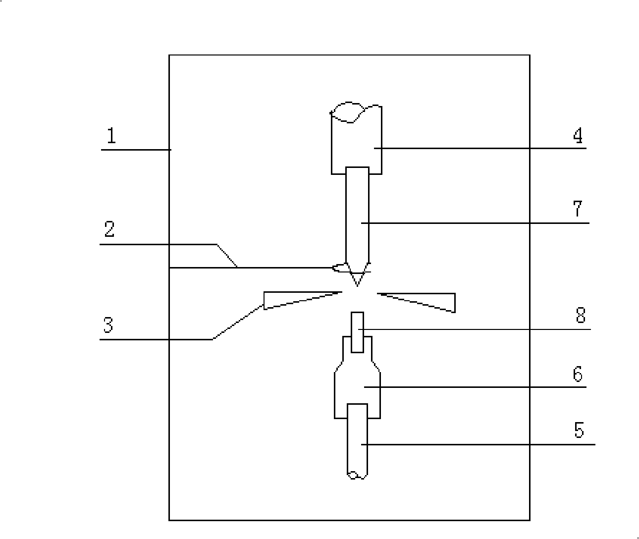
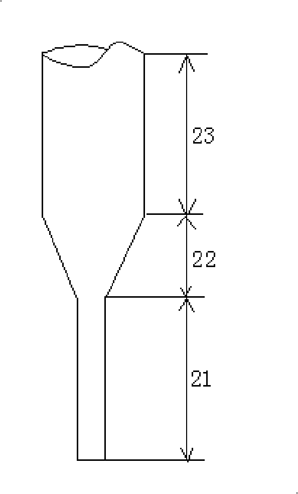
[0038] Combine now figure 1 and figure 2 To further describe this method:

[0039] The preparation method of the high-resistance silicon single crystal melted in the vacuum zone includes two major processes of polysilicon purification and silicon single crystal crystallization in sequence, and is operated according to the following steps:

[0040] A. Polysilicon purification process: the purpose is to purify polysilicon materials to obtain 11N (that is, the purity reaches 0.99999999999 and above) high-purity polysilicon. The operation steps are:

[0041] (a) Furnace cleaning and furnace loa...

Embodiment 2

[0063] Example 2 Preparation method of vacuum zone melting high-resistance silicon single crystal with Φ53±2 mm

[0064] Using the same vacuum zone melting single crystal furnace and operation method as in Example 1, a high-resistance silicon single crystal of Φ53mm±2mm was produced, and its quality reached the SEMI standard.

[0065] The difference with embodiment 1 mainly lies in the difference of each parameter condition, specifically as follows (unspecified places are identical with embodiment 1):

[0066] A. Polysilicon purification process:

[0067] (b) Evacuation and preheating process:

[0068] (6) Start the mechanical pump to evacuate the melting single crystal furnace in the vacuum zone. When the vacuum degree in the furnace chamber reaches 10 -2 Pa, turn on the molecular pump, and pump the vacuum in the furnace chamber to 3×10 -4 pa;

[0069] Use the quartz fork 2 to preheat the polysilicon rod 7 by indirect radiation. The preheating time is 20 minutes. After th...

Embodiment 3

[0082] Example 3 Preparation method of vacuum zone melting high resistance silicon single crystal with Φ53±2mm

[0083] Using the same vacuum zone melting single crystal furnace and operation method as in Example 1, a high-resistance silicon single crystal of Φ53mm±2mm was produced, and its quality reached the SEMI standard.

[0084] The difference with embodiment 1 mainly lies in the difference of each parameter condition, specifically as follows (unspecified places are identical with embodiment 1):

[0085] A. Polysilicon purification process:

[0086] (b) Evacuation and preheating process:

[0087] (6) Start the mechanical pump to evacuate the melting single crystal furnace in the vacuum zone. When the vacuum degree in the furnace chamber reaches 10 -2 At Pa, turn on the molecular pump and pump the vacuum in the furnace chamber to 1×10 -3 Pa;

[0088] Use the quartz fork 2 to preheat the polysilicon rod 7 by indirect radiation. The preheating time is 25 minutes. After t...


PUM


Abstract

The invention discloses a method for preparing vacuum zone melting high resistant silicon single crystal, comprising the two sequential major processes: polysilicon purification and crystal forming of silicon single crystal, wherein, the process of polysilicon purification comprises the steps of cleaning fire, charging, evacuating, preheating, melting materials heat sealing, growing narrow necks, shouldering, shoulder circuiting, equating diameter, ending and repeating; the process of crystal forming of silicon single crystal comprises the steps of cleaning fire, charging, evacuating, preheating, processing of chemicals, crystal seeding, shouldering, shoulder circuiting, equating diameter, ending and blowing out. With the method of the invention adopted to prepare silicon single crystal, electric resistivity, ultra-high purity, resistivity profile, uniformity of cross-section electric resistivity and minority carrier lifetime are greatly improved; purity of the silicon single crystal is above 11N, electric resistivity reaches 8000 omega/cm-30000omega/cm, uniformity of cross-section electric resistivity is less than 15%, and minority carrier lifetime is more than 600-1000Mus, thus greatly improving performance, stability and safety of the devices while realizing mass production of vacuum zone melting high resistant silicon single crystal.

Description

technical field [0001] The invention relates to the technical field of single crystal silicon, in particular to a method for preparing a high resistance silicon single crystal. Background technique [0002] High-quality and high-purity silicon single crystal is an indispensable and important material for making various radiation detectors and photodetectors. Purifying and growing silicon single crystals in a vacuum environment can make the material reach and maintain higher purity. Therefore, fused silicon single crystal in high-resistance vacuum region is the necessary material for the development of some high-sensitivity detectors, mainly with resistivity (3~5)×10 3 Ω·cm and (1~2)×10 4 There are two specifications of Ω·cm, which can be used to develop avalanche photodiodes and PIN tube-type photodetection devices respectively. Due to the change of crystal growth conditions, it is much more difficult to grow a single crystal of molten silicon in a vacuum than in an argon...

Claims


Application Information

Patent Timeline
IPC IPC(8): C30B13/00C30B29/06C30B30/04
Inventor 吴贤富邓良平丁国江万金平阮光玉袁小武徐杰王洪亮张学东
Owner 峨嵋半导体材料研究所
Why Eureka
Try Eureka