

Semiconductor wafer cutting clamper and using method thereof
A semiconductor and fixture technology, used in semiconductor/solid-state device manufacturing, clamping, manufacturing tools, etc., can solve the problems of low production process efficiency, pollution, waste of resources, etc., and achieve high production efficiency, stable quality, and high-quality product rate. high effect
Inactive Publication Date: 2009-09-09
HENAN HONGCHANG ELECTRONICS
View PDF0 Cites 9 Cited by
- Summary
- Abstract
- Description
- Claims
- Application Information
AI Technical Summary
Problems solved by technology
[0002] In the process of semiconductor processing, it is necessary to cut the whole piece of semiconductor into small pieces of semiconductor-grains. Superimposing and cutting several whole pieces of semiconductor is an effective way to improve productivity; at present, the method used is: several pieces The semiconductor wafer is smeared with graphite components or a metal interlayer and welded on the fixture. Such a fixture with several semiconductor chips is called a crystal column; the crystal column is placed on an EDM CNC machine tool for cutting, and multiple crystals can be cut at one time. Particles; the structure of the above-mentioned fixture is that one side of the fixture has a groove, and the side after the semiconductor is stacked has a raised part that matches the groove of the fixture. This raised part is welded to the fixture groove for cutting, because of this The fixture makes such a production process have disadvantages such as low efficiency, troublesome process, pollution, waste of resources, etc.
Method used
View moreImage
Smart ImageViewing Examples

Examples
Embodiment Construction
[0013] The present invention will be further described below in conjunction with the accompanying drawings.
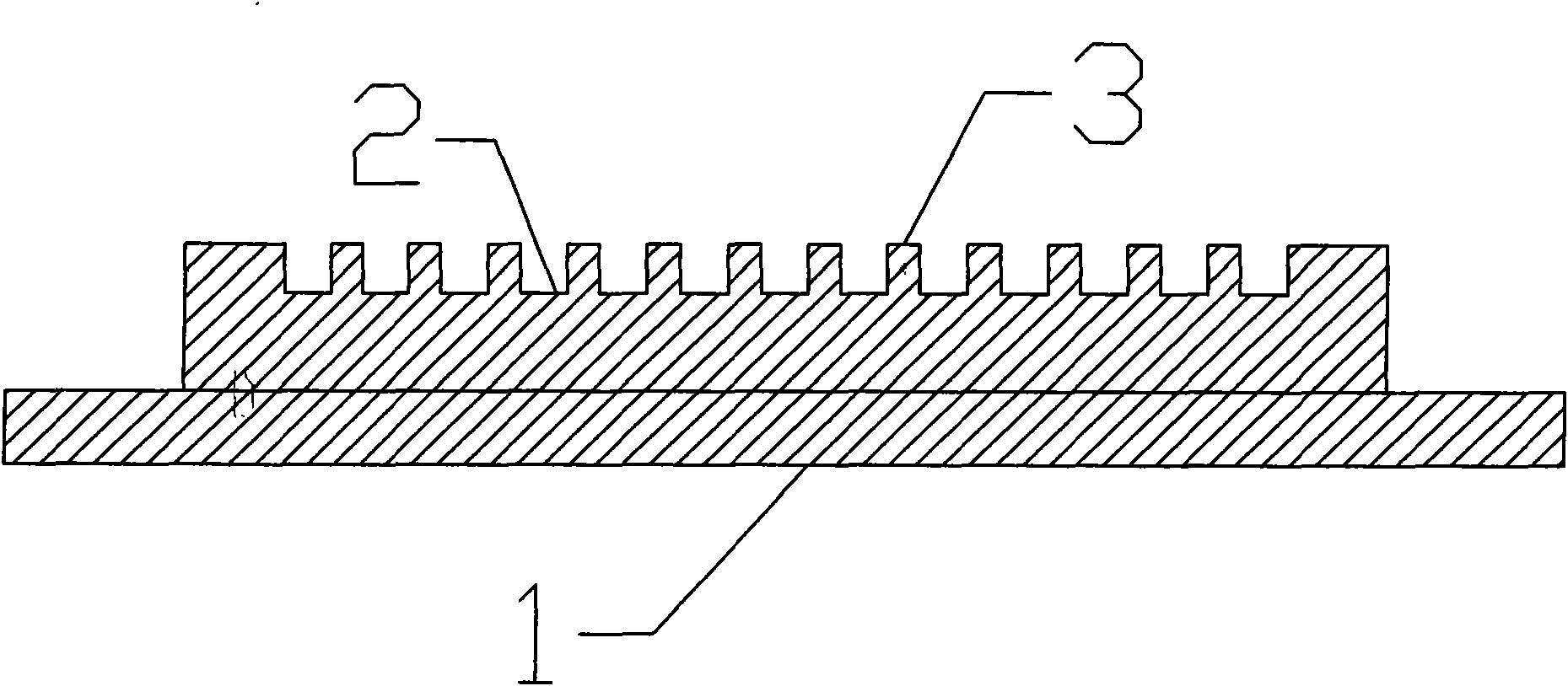
[0014] like figure 1 As shown, the semiconductor wafer cutting jig includes a jig body 1, one side of the jig body 1 has a plurality of grooves 2 engaging with a thickness of a semiconductor, and there is a protrusion 3 between the two grooves 2.
[0015] There can be 10---100 grooves.
[0016] When in use, weld or bond one side of a number of semiconductor chips to be cut to the groove 2 of the fixture body 1 to form a crystal column, and then fix the crystal column on an EDM machine tool for cutting.
[0017] Such a jig can be used to clamp semiconductor materials such as bismuth telluride for cutting.
Login to View More PUM
 Abstract
The invention belongs to the field of semiconductor processing, in particular to a semiconductor wafer cutting clamper and a using method thereof. The semiconductor wafer cutting clamper comprises a clamper body, one side of the clamper body is provided with a plurality of grooves with the thickness for engaging with a semiconductor, and a convex part is arranged between every two grooves. The method of using the clamper for cutting processing comprises clamping and the cutting of an electric spark digital-control machine tool, and is characterized in that the clamping is as following: a plurality of semiconductors are welded or adhered to the grooves of the clamper by conductive adhesive. Because the technology enables the invention to save the auxiliary material and the media required to be padded and clamped in the process of the original method, work procedures of production are reduced. Because no-graphite technology is realized, the invention has more clean and sanitary production, more environmental protection, stabler production quality, higher finished product and high-grade product rate and higher production efficiency.
Description
technical field [0001] The invention relates to the field of semiconductor processing, in particular to a semiconductor wafer cutting jig and a method for using the same. Background technique [0002] In the process of semiconductor processing, it is necessary to cut the whole piece of semiconductor into small pieces of semiconductor-grains. Superimposing and cutting several whole pieces of semiconductor is an effective way to improve productivity; at present, the method used is: several pieces The semiconductor wafer is smeared with graphite components or a metal interlayer and welded on the fixture. Such a fixture with several semiconductor chips is called a crystal column; the crystal column is placed on an EDM CNC machine tool for cutting, and multiple crystals can be cut at one time. Particles; the structure of the above-mentioned fixture is that one side of the fixture has a groove, and the side after the semiconductor is stacked has a raised part that matches the groo...
Claims
Login to View More Application Information
Patent Timeline
 Patent Type & AuthorityApplications(China)
IPC IPC(8): H01L21/68B28D7/04B23Q3/06
Inventor陈燕青陈磊
OwnerHENAN HONGCHANG ELECTRONICS