Crystal orientation and micromechanics performance measurement method of each composition crystal grain in polycrystal
A technology of crystal orientation and micromechanics, which is applied in measuring devices, scientific instruments, and material analysis through optical means, and can solve the problems of not reporting test details
- Summary
- Abstract
- Description
- Claims
- Application Information
AI Technical Summary
Problems solved by technology
Method used
Image
Examples
Embodiment 1
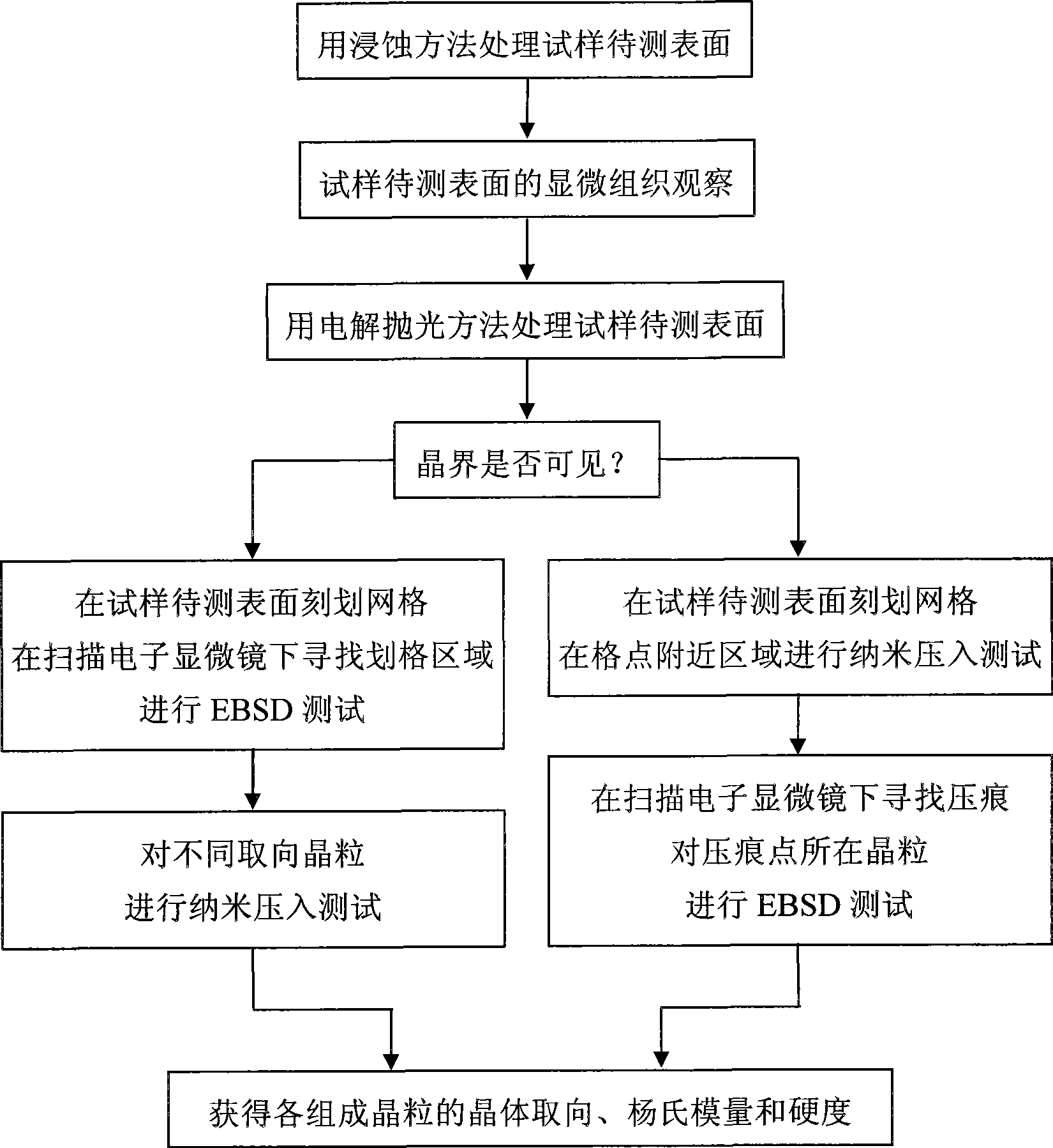
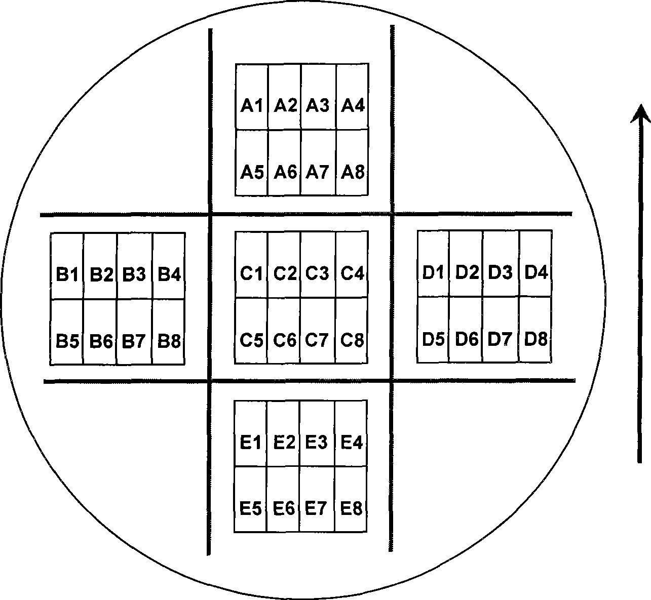
[0107] Test steps such as figure 1 As shown, the polycrystalline sample to be tested in this embodiment is industrial pure iron, and its microstructure is as follows Figure 4 As shown, the average diameter of the grains is around 300 μm. After electropolishing treatment, the grain boundaries on the surface of the sample to be tested can be clearly displayed, such as Figure 5 shown. Using a micro-nano scratch-in testing machine, use a conical scribe to scratch the surface of the sample to be tested similar to figure 2 As shown in the 5 square grids, each grid includes 8 cells, where A1~A8, B1~B8, C1~C8, D1~D8, E1~E8 are cell labels. The long side and short side dimensions of the cells are 1 mm and 0.5 mm, respectively, which are about 3 times and 2 times the average grain diameter of the sample, respectively.
[0108] Firstly, the cells to be tested are found and positioned under a scanning electron microscope, and the scanning test is performed on the area of ...
Embodiment 2
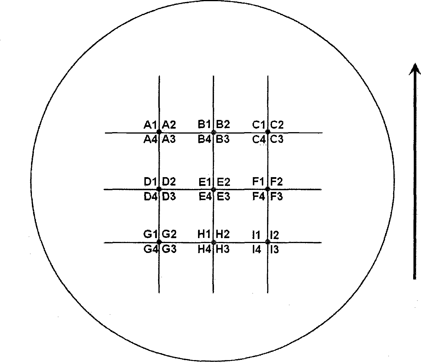
[0112] The polycrystalline sample to be tested is industrial pure copper, and its microstructure is as follows: Figure 8 As shown, the average diameter of the grains is around 200 μm. After electropolishing treatment, the grain boundaries on the surface of the sample to be tested are not displayed, such as Figure 9 shown. Use a sharp needle to manually draw a similar pattern on the surface of the sample to be tested image 3 As shown, a rectangular grid composed of 7 parallel horizontal lines and 6 mutually parallel vertical lines forms 42 grid points. Among them, A1~A4, B1~B4, C1~C4, D1~D4, E1~E4, F1~F4, G1~G4, H1~H4, and I1~I4 are grid point labels. The parallel lines are approximately 1mm apart.
[0113] First, find and locate the grid points under the optical microscope of the nanoindentation system, select the location in the area around the grid point, and set up the nanoindentation test. Fig. 10(a) shows a photograph of an indentation formed by a nanoinden...
Embodiment 3
[0118] The polycrystalline sample to be tested is super duplex stainless steel, and its microstructure is as follows Figure 12 shown. This duplex stainless steel sample has a coarse as-cast structure with well-developed dendrites. The matrix is ferrite, and the average size of austenite dendrites in the minor axis direction is about 50 μm. After electropolishing treatment, the grain boundaries on the surface of the sample to be tested can be clearly displayed, such as Figure 13 shown. Use a sharp needle to manually mark the surface of the sample to be tested similar to figure 2 In the five square grids shown, each grid includes 8, 12 or 16 cells, and the side length of each cell is about 0.5 mm, which is about 10 times the size of the austenite dendrite in the minor axis direction.
[0119] First, look for and locate the cells to be tested under a scanning electron microscope, and conduct a scanning test under EBSD on the area of each cell (including the four...
PUM
| Property | Measurement | Unit |
|---|---|---|
| radius | aaaaa | aaaaa |
| diameter | aaaaa | aaaaa |
| hardness | aaaaa | aaaaa |
Abstract
Description
Claims
Application Information


