
Radio frequency filter capable of single chip integration and manufacture method thereof

A radio frequency filter and monolithic integration technology, applied in the coupling of optical waveguides, manufacturing microstructure devices, components of TV systems, etc., to reduce substrate loss and simplify the process flow

Active Publication Date: 2009-09-16
SHANGHAI INST OF MICROSYSTEM & INFORMATION TECH CHINESE ACAD OF SCI
View PDF0 Cites 7 Cited by
  • Summary
  • Abstract
  • Description
  • Claims
  • Application Information

AI Technical Summary

Problems solved by technology

And this technology can extend the application frequency band of the filter to several GHz or higher frequency bands. At present, there are few related reports at home and abroad.

Method used


Image

  • Radio frequency filter capable of single chip integration and manufacture method thereof
  • Radio frequency filter capable of single chip integration and manufacture method thereof
  • Radio frequency filter capable of single chip integration and manufacture method thereof

Examples


Embodiment 1

[0030] Embodiment 1 - RF low-pass filter can be integrated monolithically

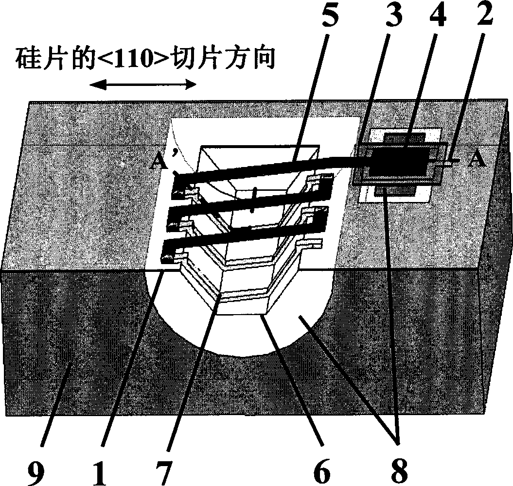
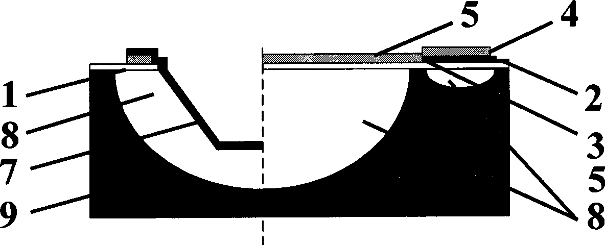
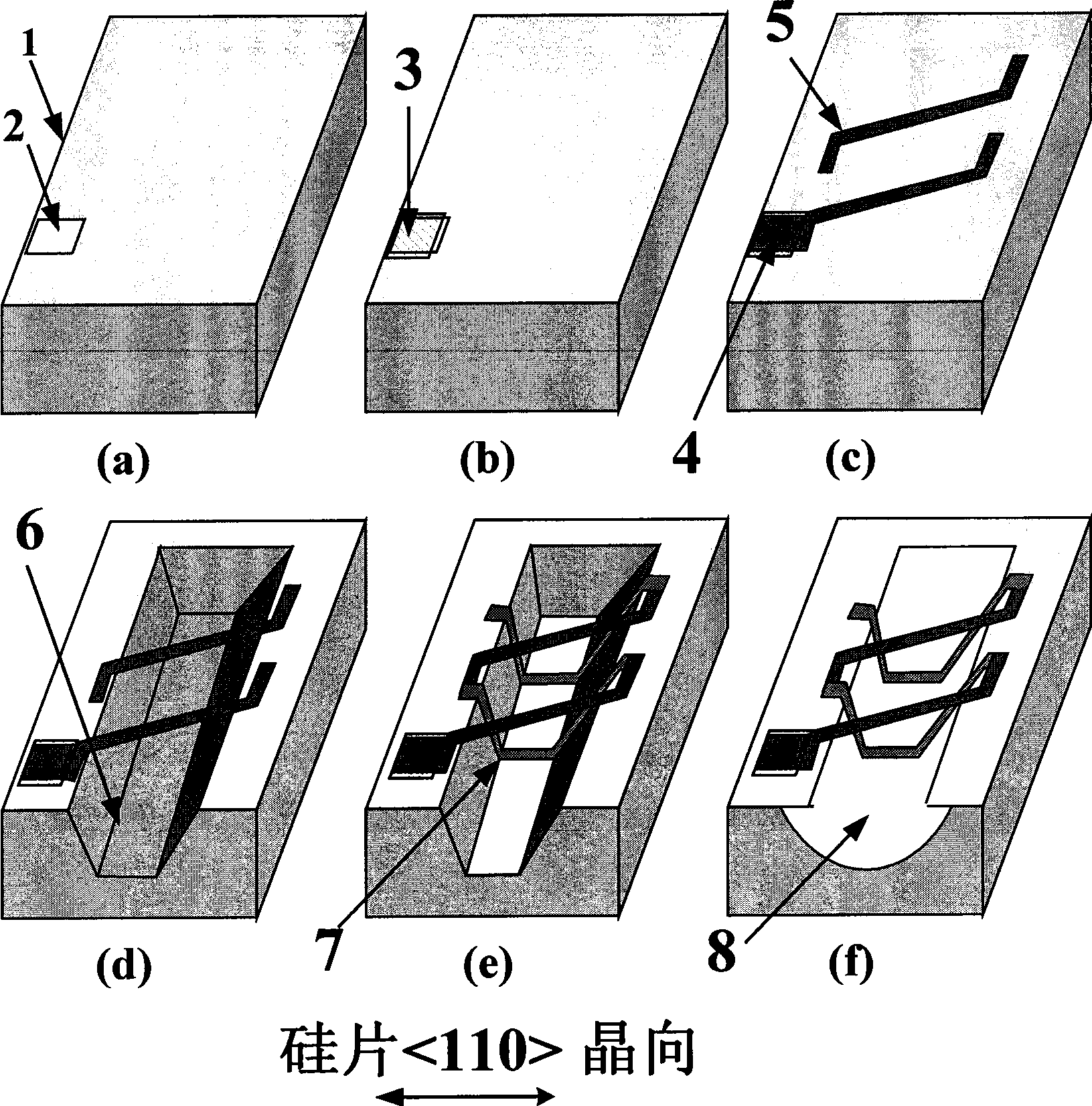
[0031] figure 1 with figure 2 Provide the present invention with a schematic structural view of an on-chip integrated radio frequency low-pass filter, figure 2 for figure 1 Cross section along AA'. A possible production implementation is as follows image 3 As shown in (a)-(f), photolithography was used 5 times in the fabrication. The implementation of this device is not limited to this process flow. In conjunction with the accompanying drawings, the description is as follows:

[0032] 1. Selected material: 4-inch double-polished P-type (100) silicon wafer, resistivity 3-8Ω·cm, thickness 450±10μm, edge cut; plasma-enhanced chemical vapor deposition (PECVD) method Form a silicon dioxide film on the surface of the silicon substrate as a supporting layer after the structure of the inductor and capacitor is released, with a thickness of 1 to 3 microns;

[0033] 2. Sputter a conductive metal laye...


PUM

PropertyMeasurementUnit
Resistivityaaaaaaaaaa
Thicknessaaaaaaaaaa
Thicknessaaaaaaaaaa

Abstract

The invention relates to a radio frequency filter capable of single chip integration and a manufacture method thereof. The radio frequency filter is characterized in that the radio frequency filter is integrated on a CMOS silicon substrate; inductor and capacitor element structures are suspended, and are embedded into the surface of a silicon chip. The method comprises the following steps that: a conductive metal layer deposited on the surface of the silicon chip is used as a lower metal electrode plate of a metal-insulating layer-metal capacitor; a growth medium layer membrane is used as an insulating medium layer of the MIM capacitor; then, an upper metal electrode plate of the MIM capacitor and an upper lead wire of an embedded screw inductor are formed while plating; a V-shaped or inverted stepped groove is formed by anisotropic etching, and is used for making a lower lead wire of the inductor and determining the opening for suspended releasing the MIM capacitor; the lower lead wire of the inductor is made in the groove of the inductor region; and finally, the inductor structure and the MIM capacitor are released by isotropic etching to be suspended. By the low temperature process, the radio frequency filter is manufactured on a common low resistance silicon chip, and the whole microprocessing manufacture process is compatible with CMOS integration circuit process.

Description

technical field [0001] The present invention relates to a monolithically integrated radio frequency filter and a method of micromachining. The radio frequency filter adopts a low-temperature process and is compatible with a standard CMOS process to realize the integration of radio frequency circuits on the same silicon chip. . The invention belongs to the application field of radio frequency micromechanical devices and circuit technology. Background technique [0002] With the application of radio frequency communication technology more and more widely, further integration and miniaturization of radio frequency front-end circuits are required. This trend makes many research work focus on a key field of radio frequency circuit integration - the integration and miniaturization of radio frequency filters. chemical research. Combined with silicon micromachining technology, the performance of passive devices and passive circuit networks on standard CMOS (complementary metal oxi...

Claims


Application Information

Patent Timeline
IPC IPC(8): H03H7/00B81B7/02H03H3/00B81C1/00
Inventor 李昕欣吴争争顾磊
Owner SHANGHAI INST OF MICROSYSTEM & INFORMATION TECH CHINESE ACAD OF SCI
Learn More