Laser peeling method of gallium nitride-based epitaxial film
A gallium nitride-based, laser lift-off technology, applied in chemical instruments and methods, from chemically reactive gases, crystal growth, etc., can solve the problems of low yield of high-power LEDs, achieve low-damage laser lift-off, and reduce radiation The effect of simple area and preparation method
- Summary
- Abstract
- Description
- Claims
- Application Information
AI Technical Summary
Problems solved by technology
Method used
Image
Examples
Embodiment 1
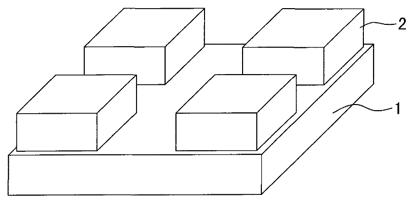
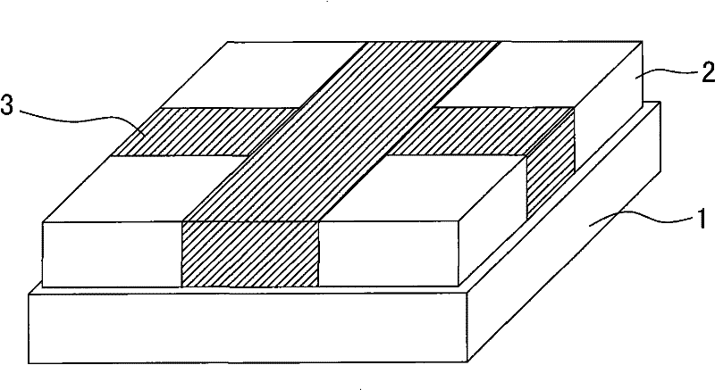
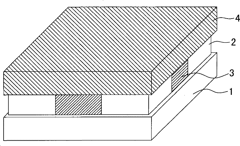
[0030] See attached Figure 1~6 As shown, a laser lift-off method of a gallium nitride-based epitaxial film comprises the following steps:
[0031] (1) if figure 1 As shown, a gallium nitride-based epitaxial film 2 is grown on a sapphire substrate 1, and then dicing grooves are made by photolithography, etching and other processes to separate and form gallium nitride-based unit devices, and the scribing grooves are scribed to the sapphire substrate The surface of the bottom 1 completely isolates the gallium nitride-based unit device; a p-electrode ohmic contact is formed on the top of the gallium nitride-based epitaxial film 2, and then a mirror is formed, and the mirror is composed of a multilayer film, such as Ti / Ag / Ti / Au, etc.;
[0032] (2) Fill the protective material 3 in the dicing groove to completely isolate the gallium nitride-based epitaxial film 2, and the filled protective material is parallel to or higher than the top of the gallium nitride chip, such as fig...
Embodiment 2
[0038] A laser lift-off method for a gallium nitride-based epitaxial film, comprising the steps of:
[0039] (1) growing GaN-based epitaxial film on sapphire substrate;
[0040] (2) Using glue or paraffin as an intermediate layer, the above-mentioned GaN-based epitaxial film is connected to a glass or Si substrate; the glue is silica gel or epoxy resin;
[0041](3) Shaping the laser spot, processing the spot projected on the interface between the sapphire substrate and the GaN-based epitaxial film into a patterned spot array; the spot diameter of the patterned spot array is 5-200 μm, and the cycle is 10 ~200μm, and its spot energy is flat-top, Gaussian or near-Gaussian distribution;
[0042] (4) irradiating the above-mentioned patterned light spot array through sapphire to the interface between the sapphire substrate and the gallium nitride, so that the gallium nitride at the interface is decomposed, and the gallium nitride-based epitaxial film is separated from the sapphire ...
PUM
| Property | Measurement | Unit |
|---|---|---|
| diameter | aaaaa | aaaaa |
Abstract
Description
Claims
Application Information


