Laser direct-write photoetching system based on photon sieve

A laser direct writing and lithography system technology, applied in the field of laser direct writing lithography, can solve the problems of incompatibility, low production efficiency, unable to meet the needs of large-scale production, etc., and achieve high resolution, high production efficiency and low cost Effect

Inactive Publication Date: 2009-10-21
INST OF OPTICS & ELECTRONICS - CHINESE ACAD OF SCI
View PDF0 Cites 26 Cited by
  • Summary
  • Abstract
  • Description
  • Claims
  • Application Information

AI Technical Summary

Problems solved by technology

The emergence of electron beam lithography, ion beam lithography, atomic lithography and other technologies based on charged particle lithography has greatly improved the resolution, which can theoretically reach about 5-10nm, but there are still some key techn

Method used


Image

  • Laser direct-write photoetching system based on photon sieve
  • Laser direct-write photoetching system based on photon sieve
  • Laser direct-write photoetching system based on photon sieve

Examples


Embodiment Construction

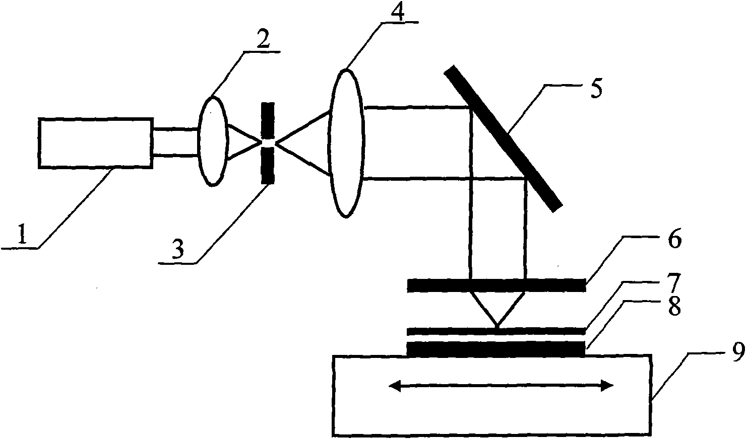
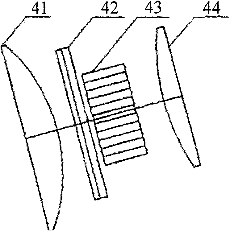
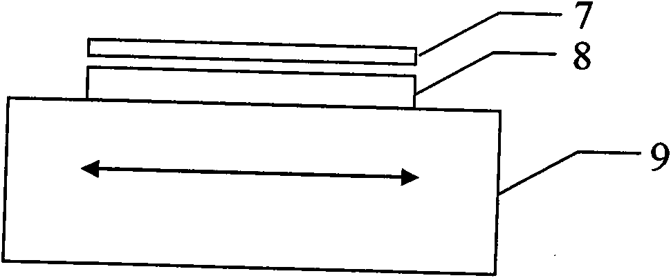
[0017] like figure 1 As shown, the present invention includes an exposure light source 1, a lens 2, a spatial filter device 3, a uniform collimation lens group 4, a mirror 5, a photon sieve 6, a photoresist 7, a substrate 8 and a scanning workpiece table 9, and the substrate 8 Placed on the scanning workpiece table 9; after the exposure light source 1 is gathered by the lens 2, it becomes uniformly collimated parallel light after passing through the spatial filter device 3 and the uniform collimation lens group 4, and then reflected by the reflector 5 onto the photon sieve 6, The photonic sieve has good focusing ability and focuses on the substrate 8 coated with photoresist 7. The scanning workpiece table 9 is an X, Y precision workpiece table. The precision workpiece table is realized according to the position and structure data of the required photolithography pattern provided by the computer. Precise control of the relative motion between the photonic sieve and the substrat...


PUM


Abstract

The invention relates to a laser direct-write photoetching system based on a photon sieve, which consists of an exposure light source (1), a lens (2), a spatial filtering device (3), a uniform collimating lens group (4), a reflector (5), the photon sieve (6), a photoresist (7), a substrate (8) and precise workpiece platforms (9). The laser light source becomes uniform and collimating parallel light after passing through the lens, the spatial filtering device and the uniform collimating lens group, the collimating parallel light irradiates the photon sieve, and the photon sieve has excellent focusing capability and focalizes on the substrate coated with the photoresist. The substrate is placed on X and Y precise workpiece platforms to achieve the required photoetching patterns by using the relative motion between the photon sieve and the substrate. The laser direct-write photoetching system has good process compatibility, the structure of the whole system is not needed to be changed; and only by changing a focusing element into a photon sieve device, the nano-scale resolving power can be achieved by using the conventional i ling and g line laser direct-write photoetching system. If the wavelength of the exposure light source is further shortened on the basis, higher resolving power can be achieved, and the nano-scale patterns can be made with ultra-low cost.

Description

technical field [0001] The invention relates to a photon sieve-based laser direct writing photolithography system, which belongs to the technical field of laser direct writing photolithography used in the manufacture of nanoscale devices in the optical microfabrication technology. Background technique [0002] In recent years, guided by advanced nano-processing technology, driven by huge market demand for information security, optoelectronic devices, biochips, communication equipment, radar, missiles, artificial satellites, etc., the field of nano-scale manufacturing technology has developed rapidly and has a wide variety Advanced nano-devices continue to come out, so that many difficult problems in the past have a solution. However, as the integration level of the semiconductor industry increases year by year, people's requirements for the resolution of lithography equipment used for nanoscale device fabrication are also getting higher and higher. Traditional proximity / con...

Claims


Application Information

Patent Timeline
IPC IPC(8): G03F7/20G03F7/004
Inventor 蒋文波胡松赵立新邢薇杨勇严伟周绍林陈旺富徐锋张博
Owner INST OF OPTICS & ELECTRONICS - CHINESE ACAD OF SCI
Why Eureka
Try Eureka