Method for flattening medium surface in heterojunction bipolar transistor (HBT) process

A planarization and dielectric technology, which is applied in the field of compound semiconductor devices and integrated circuit manufacturing processes, can solve problems affecting device yields, and achieve the effects of avoiding instability, improving yields, and improving consistency

Active Publication Date: 2009-10-21
INST OF MICROELECTRONICS CHINESE ACAD OF SCI
View PDF0 Cites 3 Cited by
  • Summary
  • Abstract
  • Description
  • Claims
  • Application Information

AI Technical Summary

Problems solved by technology

This non-planar connection ca

Method used


Image

  • Method for flattening medium surface in heterojunction bipolar transistor (HBT) process
  • Method for flattening medium surface in heterojunction bipolar transistor (HBT) process
  • Method for flattening medium surface in heterojunction bipolar transistor (HBT) process

Examples


Embodiment Construction

[0044] In order to make the object, technical solution and advantages of the present invention clearer, the present invention will be described in further detail below in conjunction with specific embodiments and with reference to the accompanying drawings.

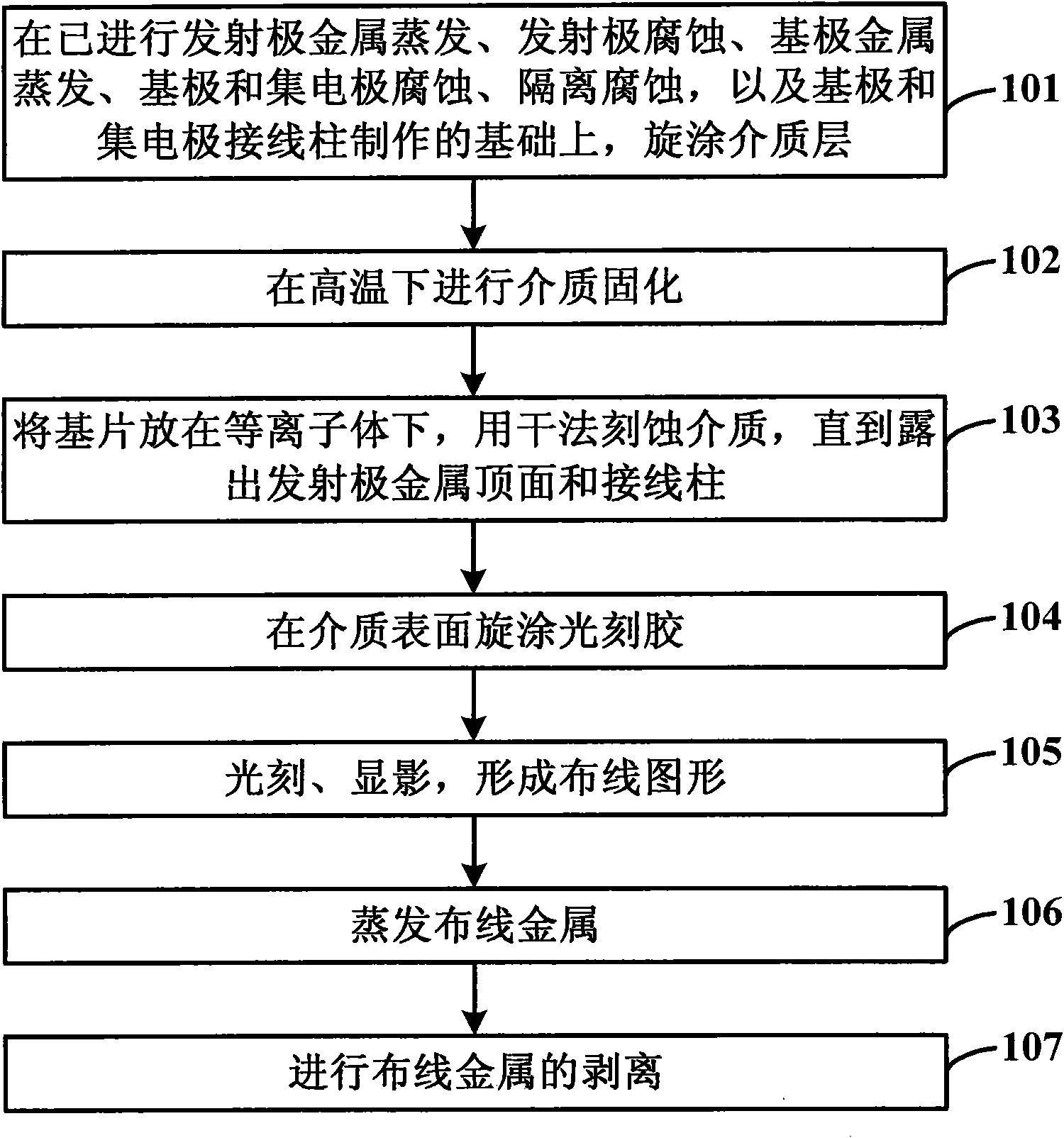
[0045] Such as figure 1 as shown, figure 1 The flow chart of the method for flattening the medium plane in the HBT process provided by the present invention, the method includes the following steps:

[0046] Step 101: spin coating a dielectric layer on the basis of the emitter metal evaporation, emitter corrosion, base metal evaporation, base and collector corrosion, isolation corrosion, and base and collector binding posts;

[0047] Step 102: performing medium curing at high temperature;

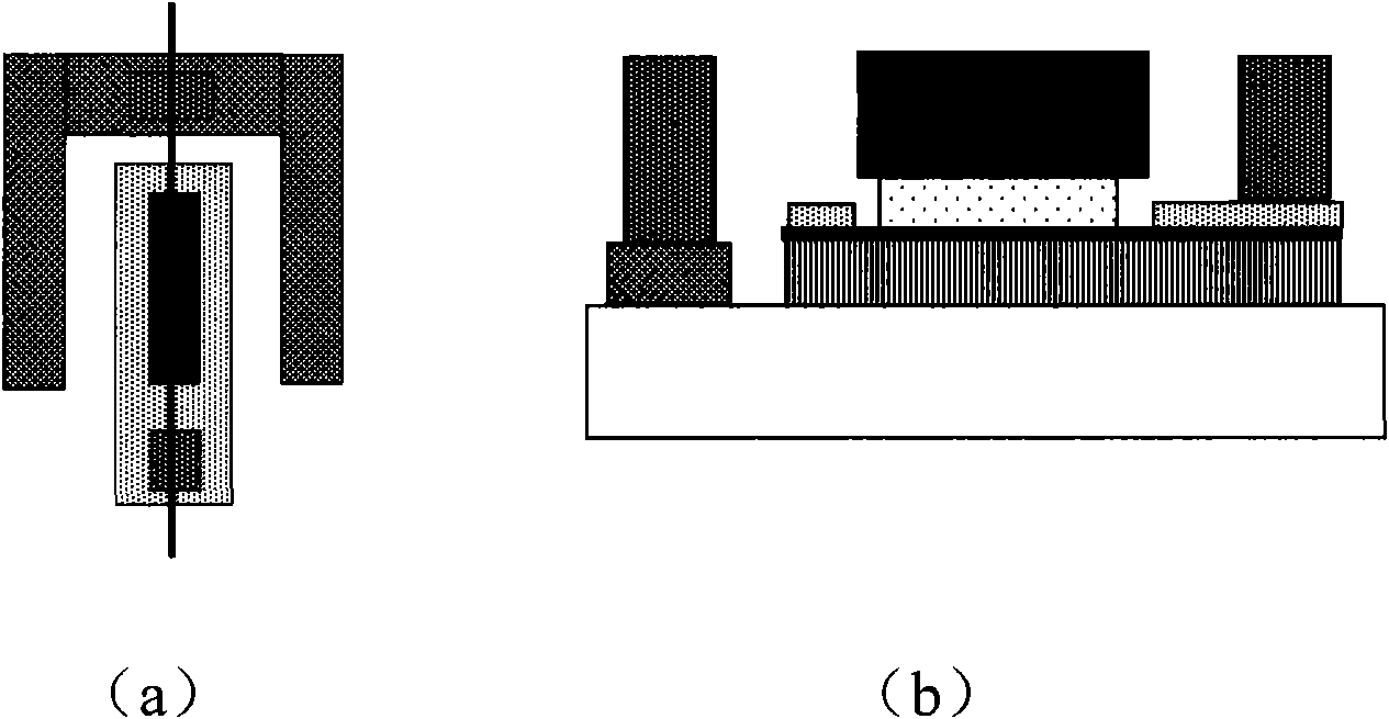
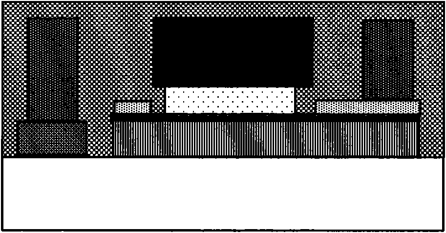
[0048] Step 103: Put the substrate under the plasma, etch the medium by dry method until the top surface of the emitter metal and the terminal are exposed;

[0049] Step 104: Spin-coat photoresist on the surface of the medium;

[0...


PUM

PropertyMeasurementUnit
Thicknessaaaaaaaaaa
Thicknessaaaaaaaaaa
Thicknessaaaaaaaaaa

Abstract

The invention relates to a method for flattening a medium surface in a heterojunction bipolar transistor (HBT) process, comprising the steps: A. coating a medium layer in a spin mode on the basis of vaporizing emitter metal, corroding an emitter, vaporizing basal pole metal, corroding and respectively corroding a basal pole and a collector and manufacturing binding posts of the basal pole and the collector; B. solidifying a medium at high temperature; C. placing a substrate under a plasma and etching the medium by a dry process until the top surface and the binding post of the emitter metal are exposed; D. coating photoresist on the surface of the medium in the spin mode; E. photoetching and developing the photoresist to form a wiring figure; F. vaporizing wiring metal; and G. peeling the wiring metal. By using the invention, the yield of a device can be effectively improved, the instability for manufacturing a micro airbridge is prevented, and the method has a great function on improving the property consistency of the device.

Description

technical field [0001] The invention relates to the technical field of compound semiconductor device and integrated circuit manufacturing technology, in particular to a method for flattening a dielectric plane in a heterojunction bipolar transistor (Heterojunction Bipolar Transistor, HBT) process. Background technique [0002] In order to improve the frequency characteristics of HBT, the size of HBT devices is getting smaller and smaller, and the connection and extraction of electrodes are becoming more and more difficult. On the one hand, in order to perform DC and high-frequency measurements of HBTs, small-sized HBTs must be connected to larger peripheral pads; on the other hand, connections between HBTs and between HBTs and passive devices are required in the circuit. As the size of the HBT decreases, the parasitics at the connection need to be considered in detail. The connection of small-sized HBT usually adopts the method of micro-air bridge or non-planar planarizatio...

Claims


Application Information

Patent Timeline
IPC IPC(8): H01L21/331
Inventor 金智刘新宇
Owner INST OF MICROELECTRONICS CHINESE ACAD OF SCI
Why Eureka
Try Eureka