Check patentability & draft patents in minutes with Patsnap Eureka AI!

Photoetching machine wafer stage dual-stage switching system

A technology for exchanging systems and wafer stages, which is applied in the field of dual-stage exchanging systems for lithography machine wafer stages, can solve the problems of non-centroid drive, high processing and assembly precision, etc., and achieve lower requirements for installation accuracy and unsatisfactory dimensional consistency requirements The effect of improving and simplifying the structure of the control system

Active Publication Date: 2009-11-04
TSINGHUA UNIV +1
View PDF3 Cites 20 Cited by
  • Summary
  • Abstract
  • Description
  • Claims
  • Application Information

AI Technical Summary

Problems solved by technology

[0008] Aiming at the deficiencies and defects of the prior art, the purpose of the present invention is to provide a new double-stage exchange system for silicon wafer stages of a lithography machine, so as to overcome the non-centroid-driven and extremely demanding processing of the existing double-stage exchange system for silicon wafer stages. And assembly accuracy and other shortcomings, so that it has the advantages of simple structure, high space utilization and no collision between the upper linear guide rails during exchange, thereby improving the exposure efficiency of the lithography machine

Method used


Image

  • Photoetching machine wafer stage dual-stage switching system
  • Photoetching machine wafer stage dual-stage switching system
  • Photoetching machine wafer stage dual-stage switching system

Examples


Embodiment Construction

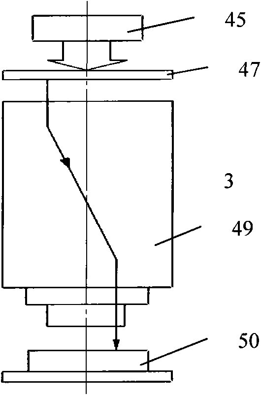
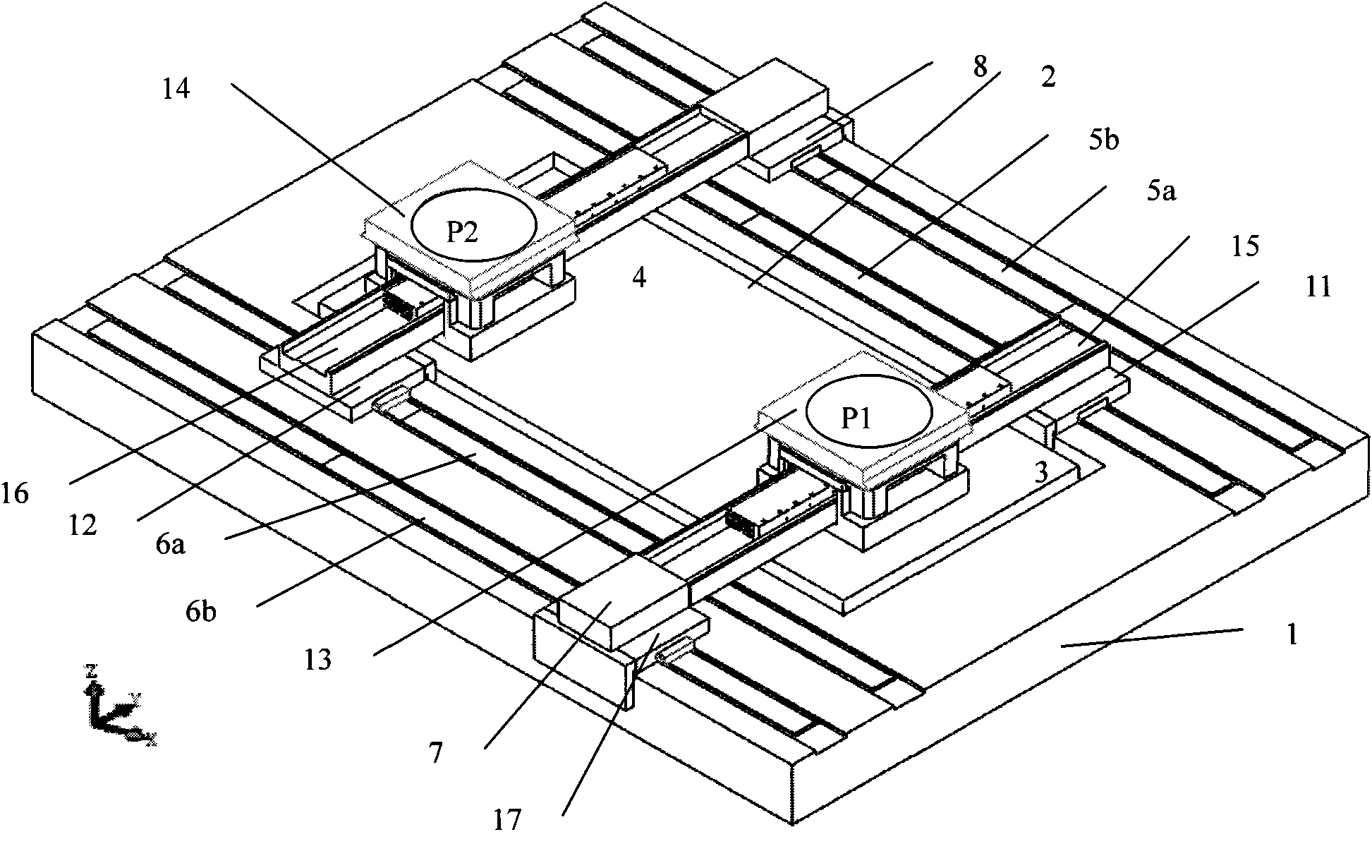
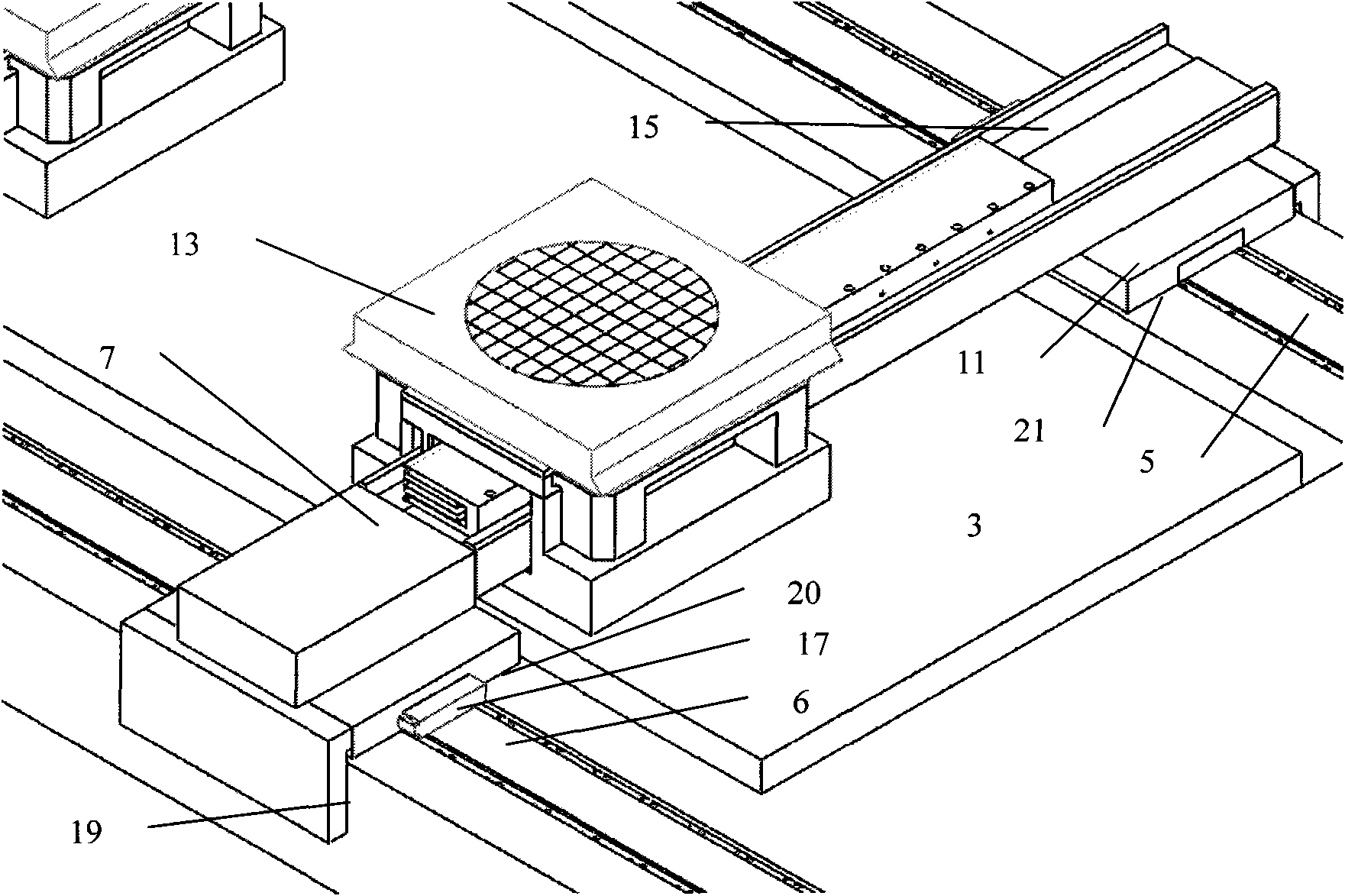
[0023] figure 2 It shows the structural schematic diagram of the dual wafer stage exchange system of the lithography machine. The system includes two wafer stages set on the same rectangular base 1, the long side is in the X direction, and the short side is in the Y direction. The two wafer stages are located at On the upper surface 2 of the base platform, the first Y-direction linear motor stator 5a, the second Y-direction linear motor stator 6a, the third Y-direction linear motor stator 5b and the fourth Y-direction linear motor stator 5b are respectively arranged on the two long side edges of the base platform. The motor stator 6b, the second single degree of freedom auxiliary drive unit 8 uses the first Y direction linear motor stator 5a, the first main drive unit 11 uses the second Y direction linear motor stator 5b, and the second main drive unit 12 uses the third Y direction The linear motor stator 6a, the fourth single-degree-of-freedom auxiliary drive unit 10 uses th...


PUM


Abstract

The invention provides a photoetching machine wafer stage dual-stage switching system which comprises a wafer stage running on an exposure working position and a wafer stage running on a pretreatment working position; the two wafer stages are arranged on a base station and suspended on the upper surface of the base station by an air bearing; each wafer stage is passed through by a lead rail along a Y direction; one end of the lead rail is connected with a master drive unit; the two wafer stages can move in the Y direction along the lead rail; the other end of the lead rail can be in abutting joint with an X direction unidirection auxiliary drive unit; and the movement of the wafer stages in the X direction is realized under the drive of the unidirection auxiliary drive unit; the unidirection auxiliary drive unit and the Y direction lead rail can separate and be in abutting joint precisely so as to realize the position switching of the two wafer stages. The system avoids the defects that when the wafer stages switch, the air bearing steps across a guide face to switch to give rise to the accuracy requirement of dimensional uniformity of the skyscraping wafer stages and high accuracy of processing and assembling of spare parts, thus greatly simplifying the system structure; in addition, the system is driven by adopting a center of mass so that the accuracy of the system is greatly increased.

Description

technical field [0001] The invention relates to a double-swap exchange system for silicon wafer tables of a lithography machine. The system is applied to a semiconductor lithography machine and belongs to the technical field of semiconductor manufacturing equipment. Background technique [0002] In the production process of integrated circuit chips, the exposure transfer (photolithography) of the design pattern of the chip on the photoresist on the surface of the silicon wafer is one of the most important processes. The equipment used in this process is called a photolithography machine (exposure machine). The resolution and exposure efficiency of the lithography machine greatly affect the characteristic line width (resolution) and productivity of the integrated circuit chip. As the key system of the lithography machine, the motion accuracy and work efficiency of the silicon wafer ultra-precision motion positioning system (hereinafter referred to as the wafer stage) largely...

Claims


Application Information

Patent Timeline
IPC IPC(8): G03F7/20
CPCG03F7/70733
Inventor 朱煜张鸣汪劲松田丽徐登峰尹文生段广洪胡金春
Owner TSINGHUA UNIV
Features
  • R&D
  • Intellectual Property
  • Life Sciences
  • Materials
  • Tech Scout
  • Unparalleled Data Quality
  • Higher Quality Content
  • 60% Fewer Hallucinations
Learn More