Resistance memory an a method for fabricating integrated circuit with same

A technology of resistive memory and integrated circuit, applied in static memory, digital memory information, circuits, etc., can solve the problems of complex manufacturing process, affecting the performance of resistive memory, damage to the interface structure of storage medium 170, etc., to simplify the manufacturing process and process method. Flexible and controllable, good interface quality

Active Publication Date: 2009-11-04
SEMICONDUCTOR MANUFACTURING INTERNATIONAL (BEIJING) CORP
View PDF0 Cites 35 Cited by
  • Summary
  • Abstract
  • Description
  • Claims
  • Application Information

AI Technical Summary

Problems solved by technology

[0004] Moreover, the manufacturing process of the resistive memory is usually to form the lower electrode 160 in the medium layer, then oxidize the material of the lower electrode to form the storage medium 170, and then form a photomask on the storage medium 170, Expose and develop the photomask to expose the storage medium 170, deposit and form the upper electrode 180 on the storage medium, and finally remove the photomask. After the storage medium 170 is formed, the storage medium 170 is stored. Multiple times of semiconductor manufacturing processes on the medium 170 will cause unnecessary damage to the interface structure of the storage medium 170 and affect the performance of the resistive memory
[0005] Moreover, in the prior art, for an integrated circuit containing a resistive memory, the formation process of the resistive memory and the interconnection structure of other memories in the integrated circuit are separately carried out, so the manufacturing process is complicated.

Method used


Image

  • Resistance memory an a method for fabricating integrated circuit with same
  • Resistance memory an a method for fabricating integrated circuit with same
  • Resistance memory an a method for fabricating integrated circuit with same

Examples


Embodiment 1

[0043] This embodiment provides a manufacturing method of an integrated circuit containing a resistive memory, refer to the attached Figure 12 shown, including:

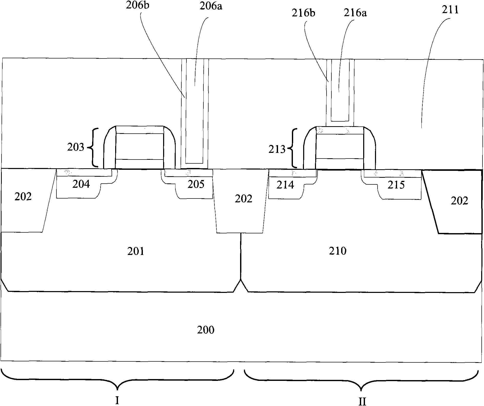
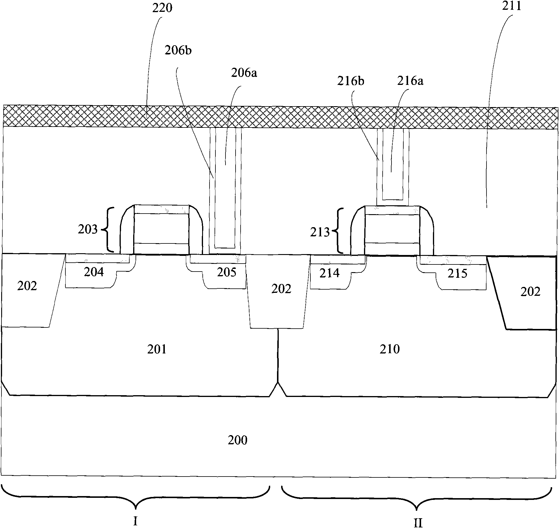
[0044] Provide a semiconductor substrate and an interlayer dielectric layer on the semiconductor substrate, the semiconductor substrate and the interlayer dielectric layer include a core device area and a peripheral circuit area;

[0045]Openings are respectively formed in the interlayer dielectric layer of the core device area and the peripheral circuit area, and barrier layers and metal wiring are filled in the openings in order to form a first interconnection structure and a second interconnection structure. The first interconnection structure is used for The second interconnect structure is used to electrically connect the semiconductor devices in the core device area, and the second interconnection structure is used to electrically connect the semiconductor devices in the peripheral circuit area;

[0046] form...

Embodiment 2

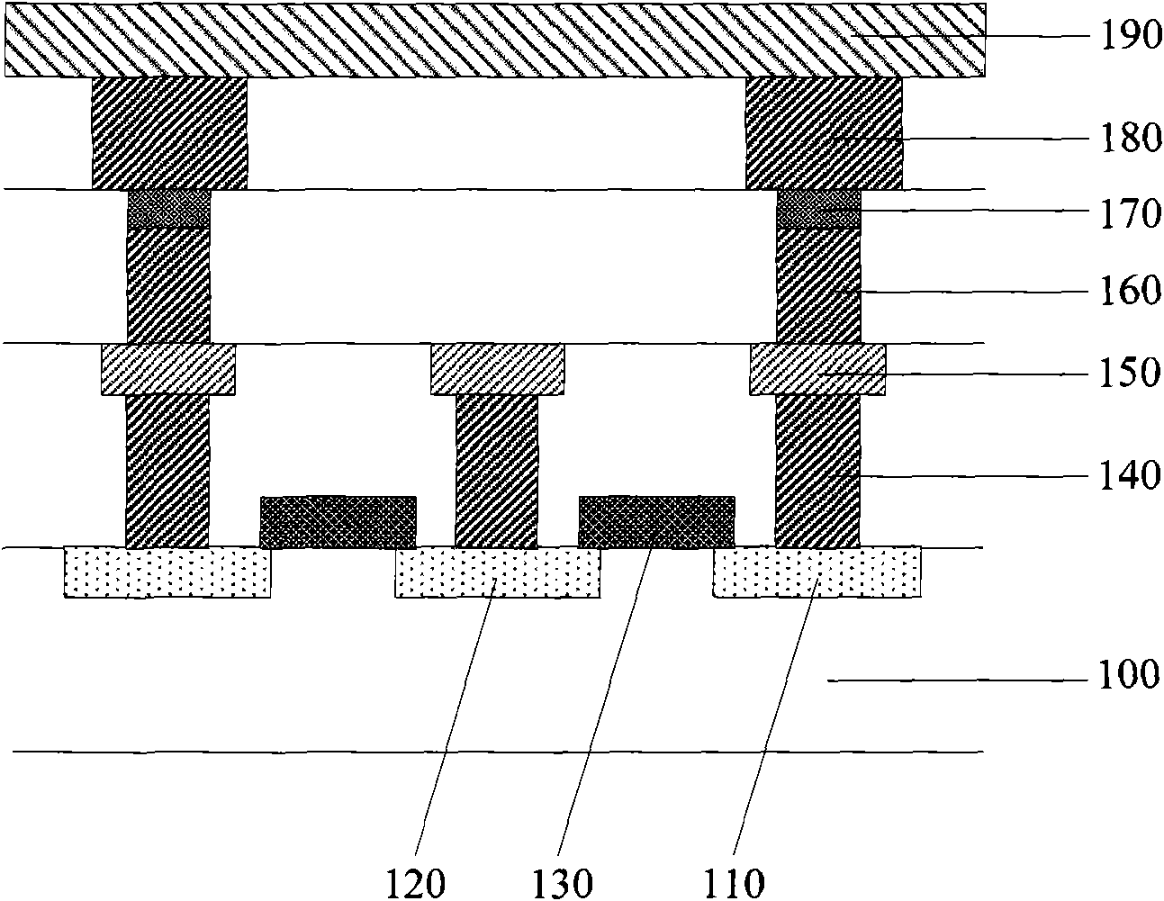
[0091] This embodiment provides a resistance memory, refer to the attached Figure 11 As shown, it includes a first interconnection structure as a lower electrode, the first interconnection structure includes a metal wiring 206a and a barrier layer 206b located on the outer sidewall of the metal wiring, and a first dielectric layer on the metal wiring 206a as a storage medium layer layer 207, an etch barrier layer 220a on the barrier layer 206b, a first conductive layer 212a on the etch barrier layer 220a and the first dielectric layer 207, and a second conductive layer 209 on the first conductive layer 212a , the first conductive layer 212a and the second conductive layer 209 constitute the upper electrode of the resistive memory.

[0092] The blocking medium layer is silicon nitride or silicon oxide or a compound structure of silicon nitride and silicon oxide, and the thickness is 20nm-80nm.

[0093] Wherein, the first interconnection structure is located in the interlayer ...


PUM

PropertyMeasurementUnit
thicknessaaaaaaaaaa
thicknessaaaaaaaaaa

Abstract

The invention relates to a method for fabricating an integrated circuit with a resistance memory, comprising the following steps: providing an interlaminar dielectric layer comprising a core component area and a peripheral circuit area; forming a first interconnection structure and a second interconnection structure which are respectively formed by a blocking layer and a metal wiring structure in the interlaminar dielectric layer; forming a blocking dielectric layer on the interlaminar dielectric layer; etching the blocking dielectric layer to expose the metal wiring structure of the core component area; forming a first dielectric layer on the metal wiring structure; forming a first conductive layer covering the blocking dielectric layer and the first dielectric layer; forming a masking film on the first conductive layer; etching the first conductive layer and the blocking dielectric layer until the second interconnecting structure is exposed; keeping the first conductive layer and a blocking dielectric layer on the first interconnecting structure; and forming a second conductive layer and a third conductive layer respectively on the first conductive layer and the second interconnecting structure. Due to the adoption of the method for fabricating the integrated circuit with the resistance memory, when the resistance memory is formed, the interlaminar interconnection structures of the core component area and the peripheral circuit area can be also formed.

Description

technical field [0001] The invention relates to the technical field of semiconductor manufacturing, in particular to a method for manufacturing a resistance memory and an integrated circuit containing the resistance memory. Background technique [0002] At present, the development of new storage technologies with low cost, high speed, high storage density, simple manufacturing and good compatibility with the current complementary metal oxide (CMOS) semiconductor integrated circuit process has attracted widespread attention worldwide. Resistive random access memory (RRAM) memory technology based on metal oxides with resistive switching characteristics is currently the focus of development by many device manufacturers, because this technology can provide higher density, lower cost and lower power consumption. power non-volatile memory. The resistance value of the RRAM memory cell will change greatly after the pulse voltage is applied, and this resistance value can still be ma...

Claims


Application Information

Patent Timeline
Patent Type & Authority Applications(China)
IPC IPC(8): H01L21/822H01L21/768H01L27/24H01L23/522H01L45/00G11C11/56G11C13/00
Inventor 鲍震雷
Owner SEMICONDUCTOR MANUFACTURING INTERNATIONAL (BEIJING) CORP
Why Eureka
Try Eureka