Resistance memory and method for fabricating integrated circuit with same

A resistive memory, integrated circuit technology, applied in static memory, digital memory information, circuits, etc., can solve the problems of complex manufacturing process, damage to the interface structure of the storage medium 170, affecting the performance of resistive memory, etc., to simplify the manufacturing process and process method. Flexible and controllable, good interface quality

Active Publication Date: 2009-11-04
SEMICONDUCTOR MANUFACTURING INTERNATIONAL (BEIJING) CORP
View PDF0 Cites 17 Cited by
  • Summary
  • Abstract
  • Description
  • Claims
  • Application Information

AI Technical Summary

Problems solved by technology

[0004] Moreover, the manufacturing process of the resistive memory is usually to form the lower electrode 160 in the medium layer, then oxidize the material of the lower electrode to form the storage medium 170, and then form a photomask on the storage medium 170, Expose and develop the photomask to expose the storage medium 170, deposit and form the upper electrode 180 on the storage medium, and finally remove the photomask. After the storage medium 170 is formed, the storage medium 170 is stored. Multiple times of semiconductor manufacturing processes on the medium 170 will cause unnecessary damage to the interface structure of the storage medium 170 and affect the performance of the resistive memory
[0005] Moreover, in the prior art, for an integrated circuit containing a resistive memory, the formation process of the resistive memory and the interconnection structure of other memories in the integrated circuit are separately carried out, so the manufacturing process is complicated.

Method used


Image

  • Resistance memory and method for fabricating integrated circuit with same
  • Resistance memory and method for fabricating integrated circuit with same
  • Resistance memory and method for fabricating integrated circuit with same

Examples


Embodiment 1

[0045] This embodiment provides a method for manufacturing an integrated circuit including a resistive memory, including:

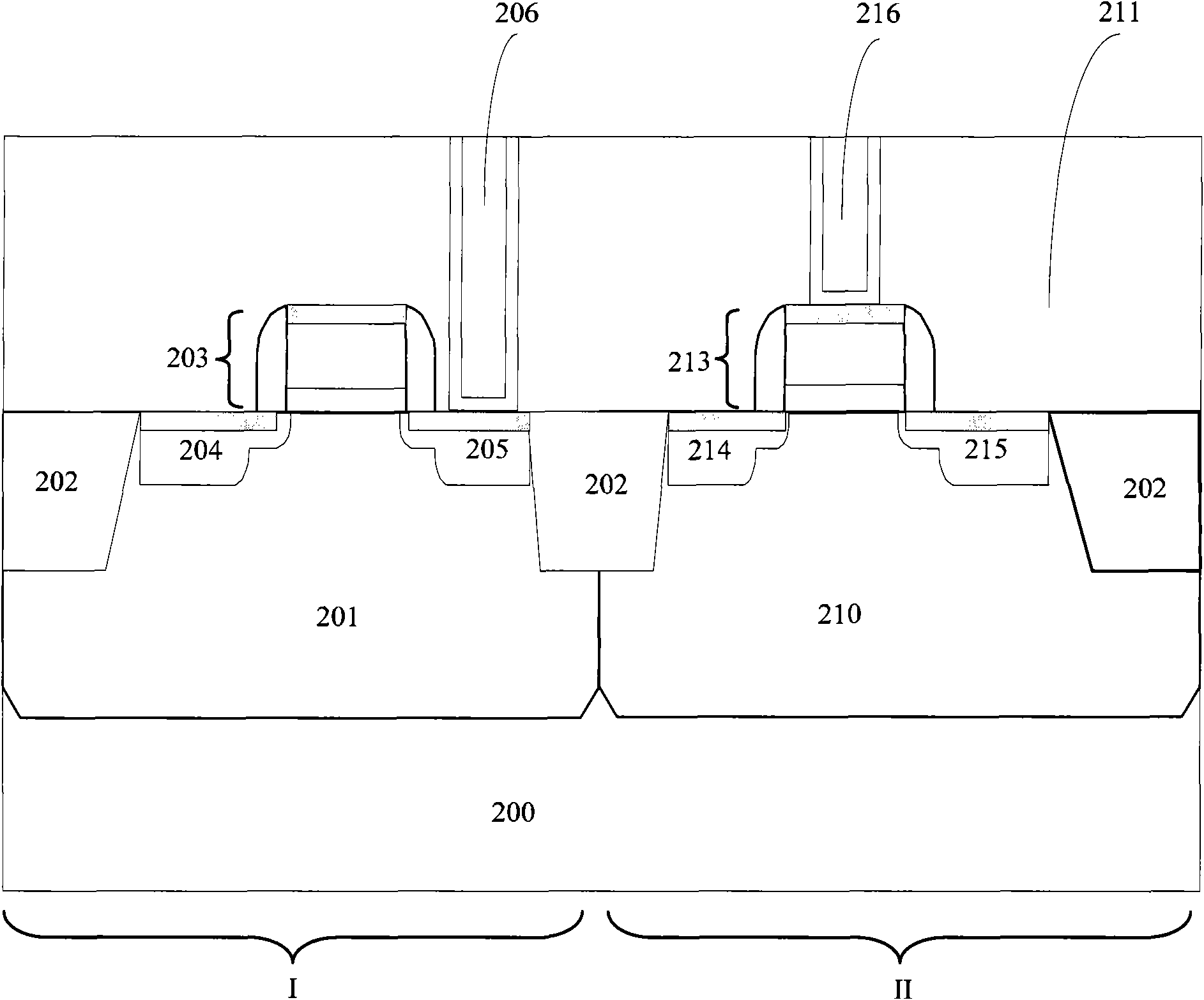
[0046] Provide a semiconductor substrate and an interlayer dielectric layer on the semiconductor substrate, the semiconductor substrate and the interlayer dielectric layer include a core device area and a peripheral circuit area;

[0047] A first interconnection structure is formed in the interlayer dielectric layer in the core device area, a second interconnection structure is formed in the interlayer dielectric layer in the peripheral circuit area, the first interconnection structure is used to electrically connect the semiconductor devices in the core device area, The second interconnection structure is used to electrically connect the semiconductor devices in the peripheral circuit area;

[0048] forming a first dielectric layer on the first interconnection structure, and forming a second dielectric layer on the second interconnection structure;

[0...

specific Embodiment approach

[0077] By adopting the first specific implementation manner, the subtle influence of the ashing process on the photoresist on the surface of the second interconnection structure is avoided, and a good surface of the second interconnection structure is maintained.

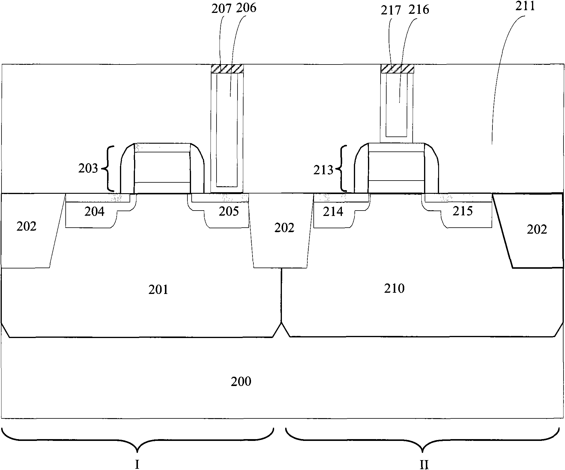
[0078] On the other hand, the first conductive layer and the second dielectric layer in the peripheral circuit area are removed to expose the second interconnection structure, and only the first conductive layer on the first dielectric layer is left in the core device area. The method can be: refer to the attached Figure 5 As shown, a mask layer 218 is formed on the first conductive layer 212. The mask layer 218 is, for example, a photoresist layer. Refer to the attached Image 6 As shown, the photoresist layer 218 is exposed and developed, the photoresist layer in the peripheral circuit region II and the photoresist layer other than the position corresponding to the first interconnection structure 206 in the core ...

Embodiment 2

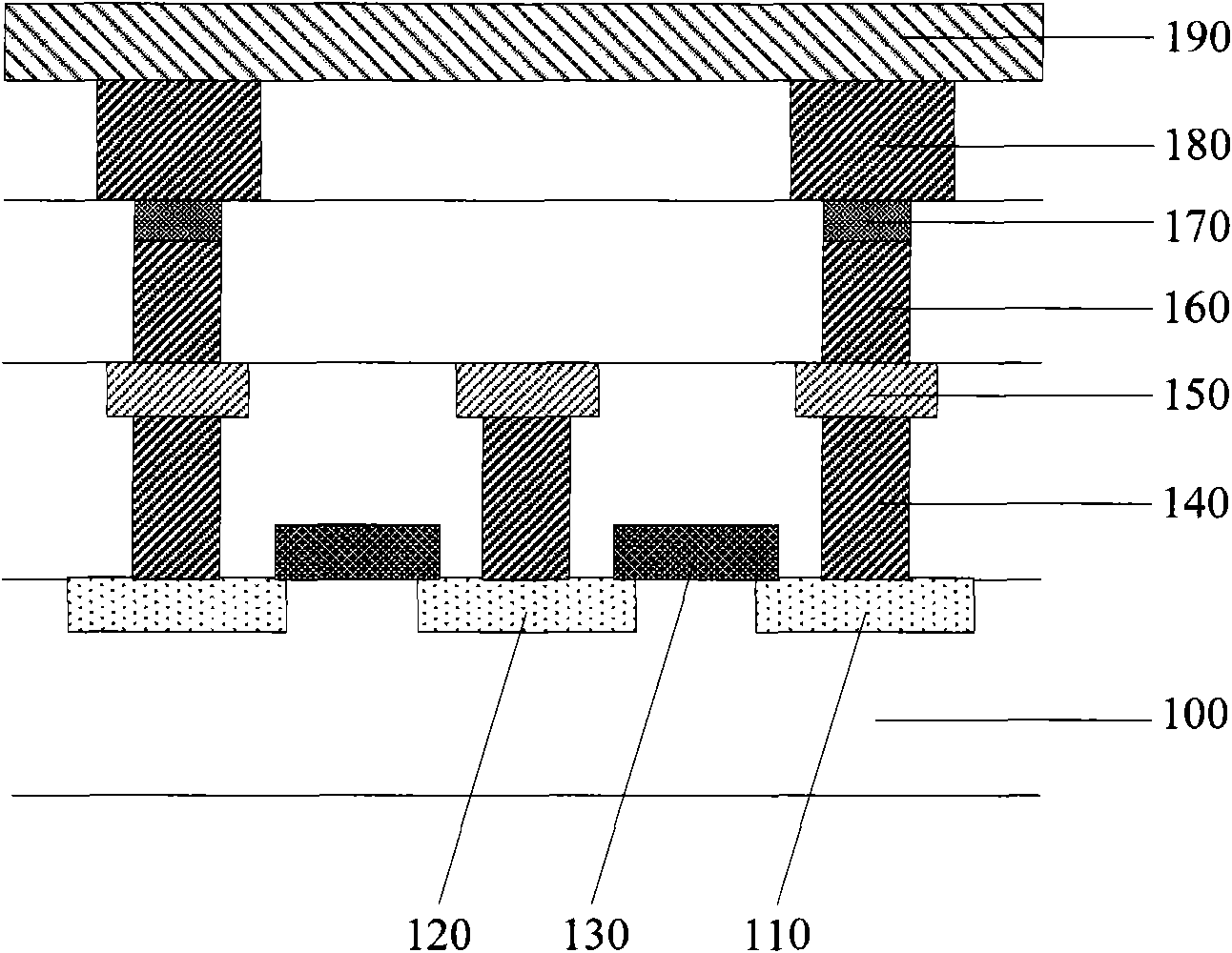
[0090] This embodiment provides a resistance memory, refer to the attached Figure 10 As shown, it includes a first interconnection structure 206 as a lower electrode, a first dielectric layer 207 as a storage medium layer, and a first conductive layer 212 and a second conductive layer 209 as an upper electrode.

[0091] Wherein, the first interconnection structure 206 is metal copper or metal tungsten, and the attached Figure 10 The second interconnection structure 216 in the peripheral circuit area of ​​the integrated circuit is formed at the same time, and the formation process is any prior art well known to those skilled in the art.

[0092] The first dielectric layer 207 may be formed by direct oxidation of the first interconnection structure 206, preferably a thermal oxidation process. Or the WO deposited directly on the first interconnection structure 206 by chemical vapor deposition or physical vapor deposition X ,TiO 2 , NiO, ZrO 2 , HfO 2 , CeO 2 , RuO X , Cu...


PUM

PropertyMeasurementUnit
thicknessaaaaaaaaaa
thicknessaaaaaaaaaa

Abstract

The invention relates to a method for fabricating an integrated circuit with a resistance memory, comprising the following steps: providing an interlaminar dielectric layer comprising a core component area and a peripheral circuit area; forming a first interconnection structure and a second interconnection structure in the interlaminar dielectric layer; respectively forming a first dielectric layer and a second dielectric layer on the surface of the first interconnection structure and on the surface of the second interconnection structure; forming first conductive layers covering the interlaminar dielectric layer, the first dielectric layer and the second dielectric layer; removing a first conductive layer and a second conductive layer on the peripheral circuit area to expose the second interconnection structure and only keeping the first conductive layer on the first dielectric layer in the core component area; and respectively forming a second conductive layer and a third conductive layer on the first conductive layer of the first dielectric layer and on the second interconnection structure. Due to the adoption of the method for fabricating the integrated circuit with the resistance memory, when the resistance memory is formed, the interlaminar interconnection structure of the core component area and the peripheral circuit area can be also formed.

Description

technical field [0001] The invention relates to the technical field of semiconductor manufacturing, in particular to a resistance memory, an integrated circuit containing the resistance memory and a manufacturing method thereof. Background technique [0002] At present, the development of new storage technologies with low cost, high speed, high storage density, simple manufacturing and good compatibility with the current complementary metal oxide (CMOS) semiconductor integrated circuit process has attracted widespread attention worldwide. Resistive random access memory (RRAM) memory technology based on metal oxides with resistive switching characteristics is currently the focus of development by many device manufacturers, because this technology can provide higher density, lower cost and lower power consumption. power non-volatile memory. The resistance value of the RRAM memory cell will change greatly after the pulse voltage is applied, and this resistance value can still ...

Claims


Application Information

Patent Timeline
Patent Type & Authority Applications(China)
IPC IPC(8): H01L21/822H01L21/768H01L27/24H01L23/522H01L45/00G11C11/56G11C13/00
Inventor 鲍震雷
Owner SEMICONDUCTOR MANUFACTURING INTERNATIONAL (BEIJING) CORP
Why Eureka
Try Eureka