

Photonic crystal vertical cavity surface emitting laser with single module, large power and low divergence angle
A technology of vertical cavity surface emission and photonic crystals, which is applied in the direction of semiconductor lasers, lasers, laser components, etc., can solve the problems of divergence angles that have not been reported, and achieve the effects of flexible device structure design, increased bandwidth, and extended life.
- Summary
- Abstract
- Description
- Claims
- Application Information
AI Technical Summary
Problems solved by technology
Method used
Image

Examples
Embodiment 1
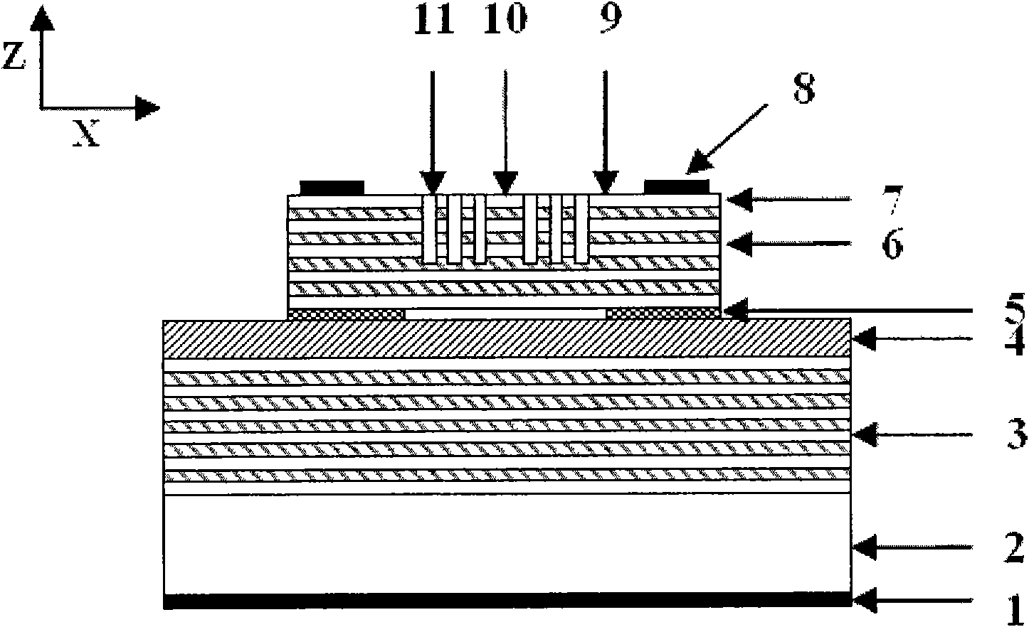
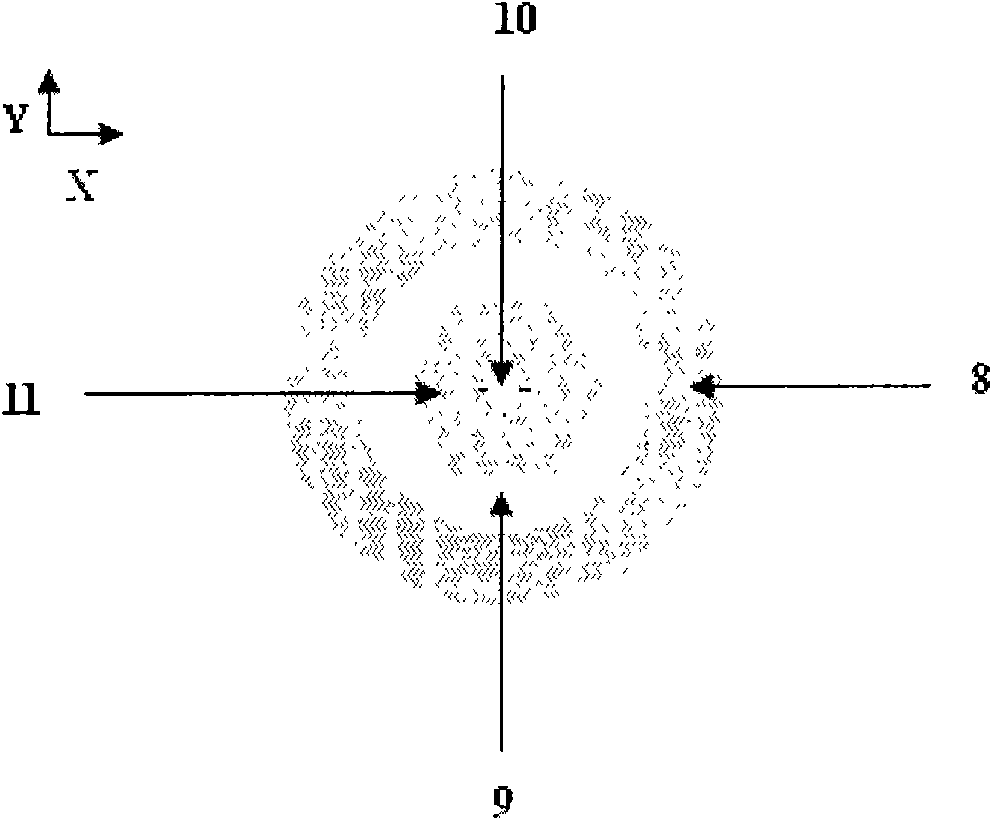
[0041]In this example, the working wavelength of the photonic crystal vertical cavity surface emitting laser with single mode, high power and low divergence angle is 0.85 μm. The schematic diagram of the surface topography of the upper DBR of the photonic crystal vertical cavity surface emitting laser of this example is as follows figure 2 shown.
[0042] In this example, the lower electrode is AuGeNiAu alloy, the upper electrode is TiAu alloy, the lower DBR is 34.5 pairs of n-type GaAs / AlGaAs, the active region is 3 pairs of GaAs quantum wells, the oxidation aperture is 34 μm, and the upper DBR is 20.5 pairs of p-type GaAs / AlGaAs; the surface of the upper DBR is engraved with a photonic crystal pattern of a single defect cavity, the period of the photonic crystal is 4 μm, the duty ratio is 0.5, and the etching depth is 10 pairs of DBR; the defect area is surrounded by a photonic crystal composed of three circles of air columns High loss region; the inner diameter of the ri...
Embodiment 2
[0045] In this example, the working wavelength of the photonic crystal vertical cavity surface emitting laser with single mode, high power and low divergence angle is 1.3 μm. Such as Figure 4 as shown, Figure 4 A top view of the surface topography of the upper DBR of the photonic crystal vertical cavity surface emitting laser provided according to the second embodiment of the present invention.
[0046] In this example, the lower electrode is AuGeNiAu alloy, the upper electrode is TiAu alloy, the lower DBR is 33.5 pairs of n-type GaAs / AlGaAs, the active region is 3 pairs of GaAs quantum wells, the oxidation aperture is 32 μm, and the upper DBR is 23 pairs of p-type GaAs / AlGaAs; the surface of the upper DBR is engraved with a photonic crystal pattern of a single defect cavity, the period of the photonic crystal is 5 μm, the duty ratio is 0.5, and the etching depth is 18 pairs of DBR; the defect area is surrounded by a photonic crystal composed of two circles of air columns ...
PUM
| Property | Measurement | Unit |
|---|---|---|
| The inside diameter of | aaaaa | aaaaa |
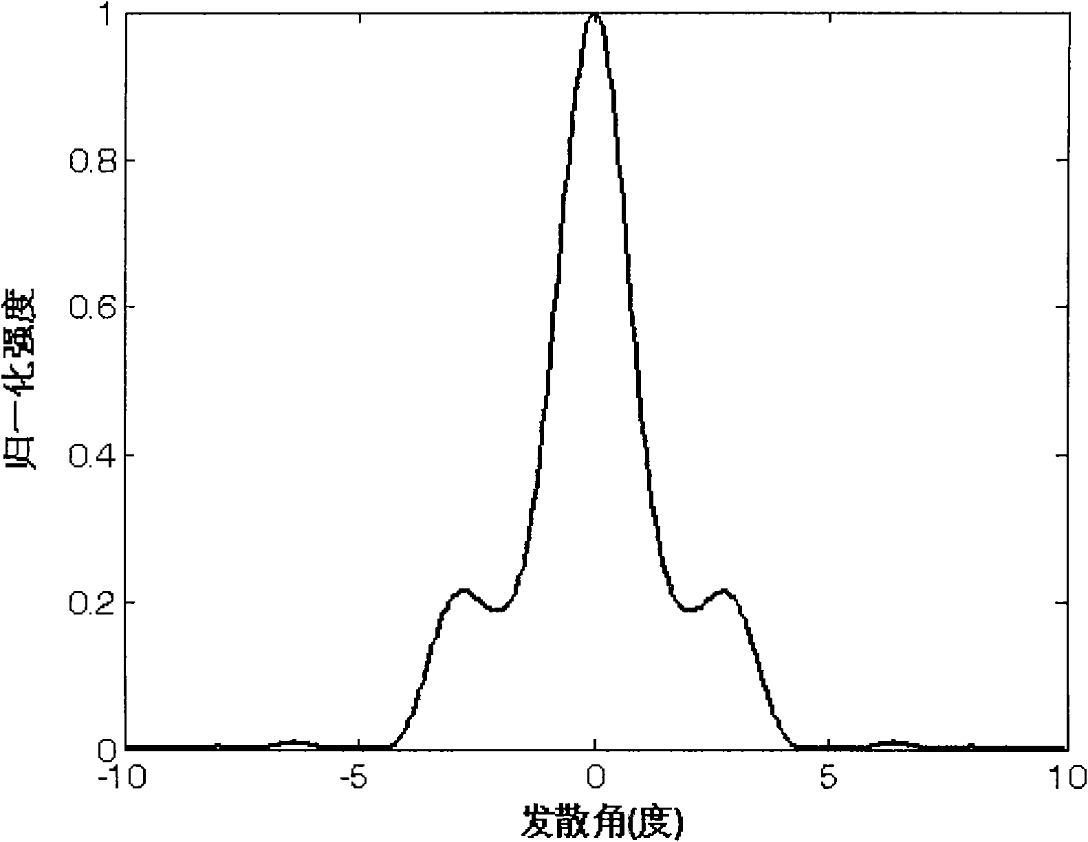
| Divergence angle | aaaaa | aaaaa |
| The inside diameter of | aaaaa | aaaaa |
Abstract
Description
Claims
Application Information