

Indium arsenide (InAs) quantum dot material modulated by covering layers of gallium arsenide (GaAs) and gallium antimonide (GaSb) and growing method thereof
A quantum dot material, gallium arsenide technology, applied in the field of indium arsenide quantum dot material and its molecular beam epitaxy growth, can solve the problem of uneven quantum dot size and deterioration of laser gain, and achieve the effect of uniform size distribution
- Summary
- Abstract
- Description
- Claims
- Application Information
AI Technical Summary
Problems solved by technology
Method used
Image

Examples
Embodiment Construction
[0026] Hereinafter, the present invention will be further described in detail with reference to the accompanying drawings.
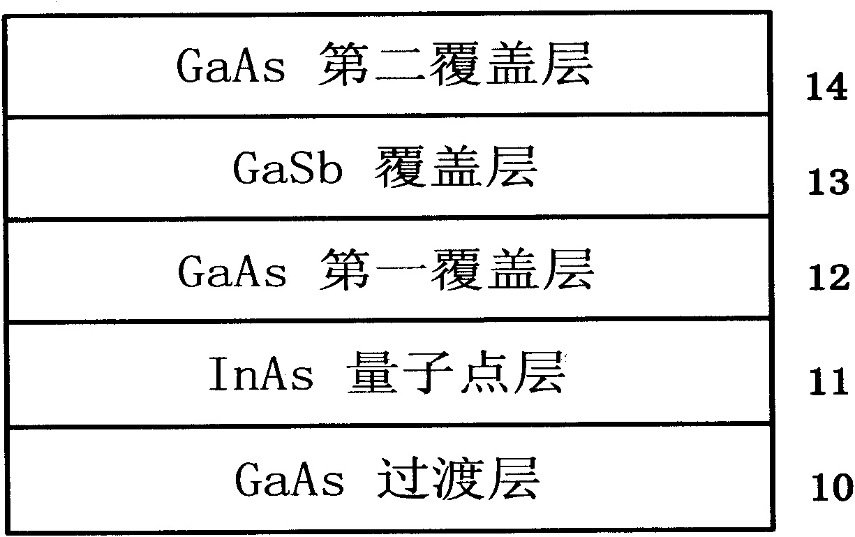
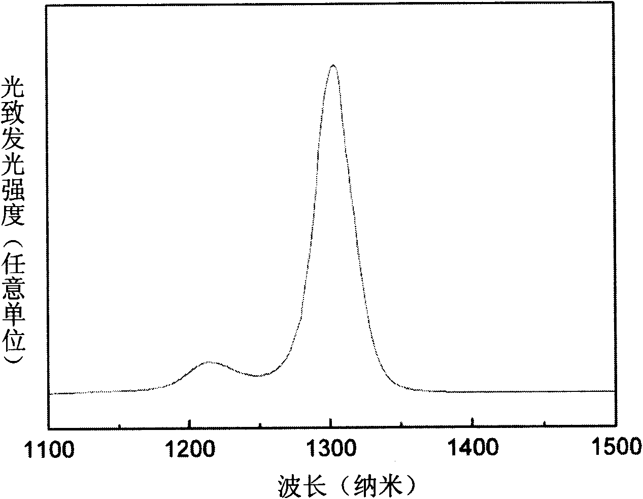
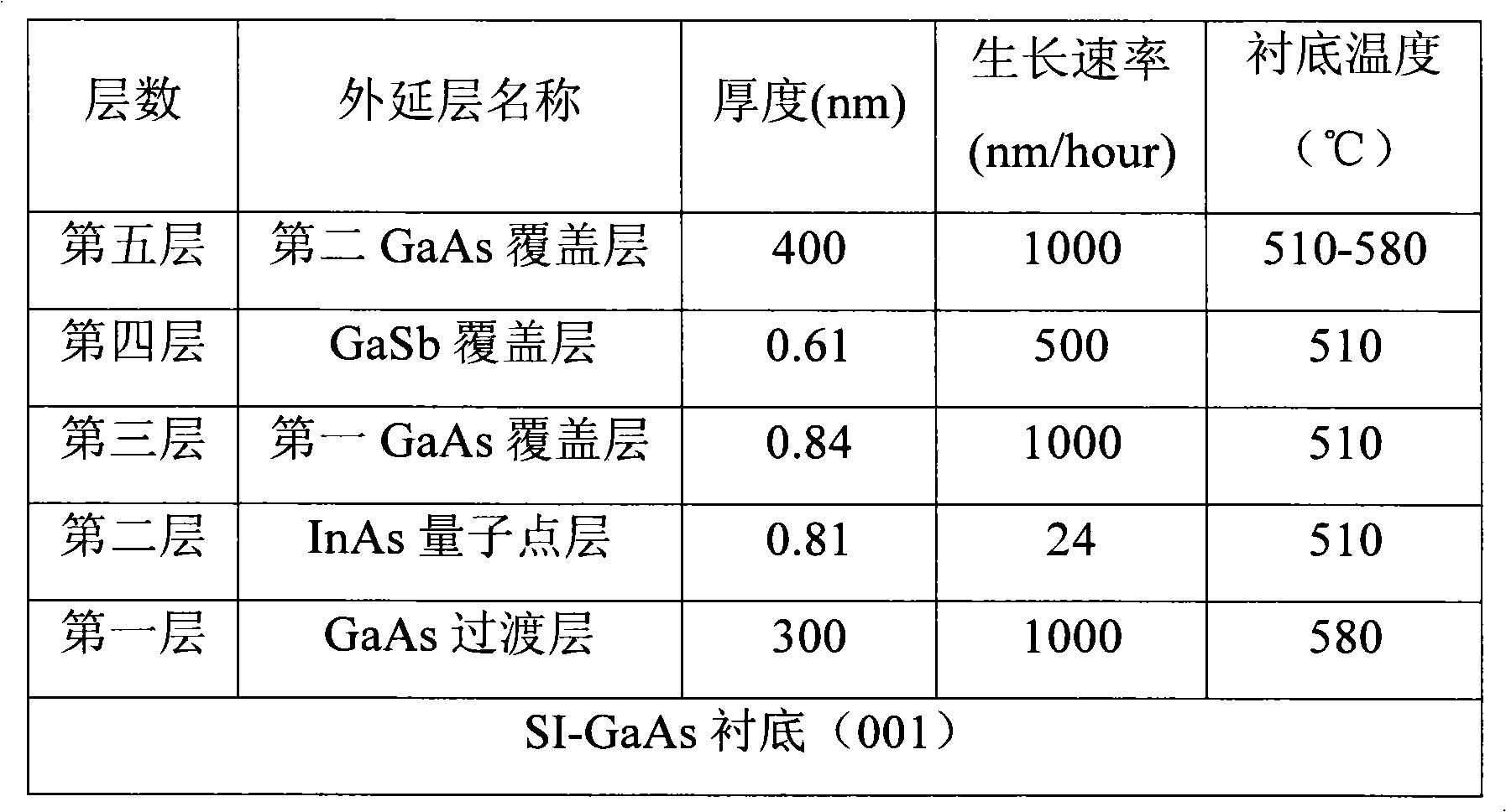
[0027] figure 1 The indium arsenide quantum dot structure modulated by gallium arsenide and gallium antimonide covering layers of the present invention is given. The structure includes a substrate on which a GaAs transition layer 10 is formed by a well-known molecular beam epitaxy method. The substrate temperature is 580°C. , The thickness of the GaAs transition layer is controlled to 500nm. Then, the InAs self-assembled quantum dot layer 11 is grown by molecular beam epitaxy on the GaAs transition layer 10, the substrate temperature is controlled to 510° C., and the thickness is preferably 0.81 nm. Then the substrate temperature was controlled to 510°C, and the first GaAs covering layer 12 was grown by molecular beam epitaxy on the InAs self-assembled quantum dot layer 11, the thickness of the covering layer 12 was 0.84 nm, and GaSb was grown on the coveri...
PUM
| Property | Measurement | Unit |
|---|---|---|
| thickness | aaaaa | aaaaa |
| thickness | aaaaa | aaaaa |
| thickness | aaaaa | aaaaa |
Abstract
Description
Claims
Application Information