Laminated dielectric layer forming method and metal foredielectric layer forming method

A technology of metal front dielectric layer and dielectric layer, which is applied in the formation of metal front dielectric layer and the formation of laminated dielectric layer, can solve the problem of losing the tensile stress of the film layer, failing to meet the stress requirements, and the stress value of the metal front dielectric layer not meeting the design Requirements and other issues to achieve the effect of avoiding the influence of device thermal stability

Inactive Publication Date: 2009-12-02
SEMICONDUCTOR MANUFACTURING INTERNATIONAL (BEIJING) CORP
View PDF1 Cites 18 Cited by
  • Summary
  • Abstract
  • Description
  • Claims
  • Application Information

AI Technical Summary

Problems solved by technology

[0007] However, the problem is that the above-mentioned first dielectric layer and second dielectric layer constituting the pre-metal dielectric layer are manufactured by different equipment. In the actual process flow, the first dielectric layer deposited by HARP SACVD process is relatively loose, and the surface layer has more Si-H dangling bonds exposed to the air are oxidized into Si-OH bonds, which makes the film easy to absorb moisture and gradually loses the tensile stress in the film layer, r...

Method used


Image

  • Laminated dielectric layer forming method and metal foredielectric layer forming method
  • Laminated dielectric layer forming method and metal foredielectric layer forming method
  • Laminated dielectric layer forming method and metal foredielectric layer forming method

Examples


Embodiment 1

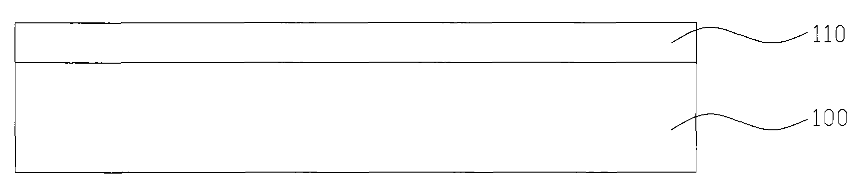
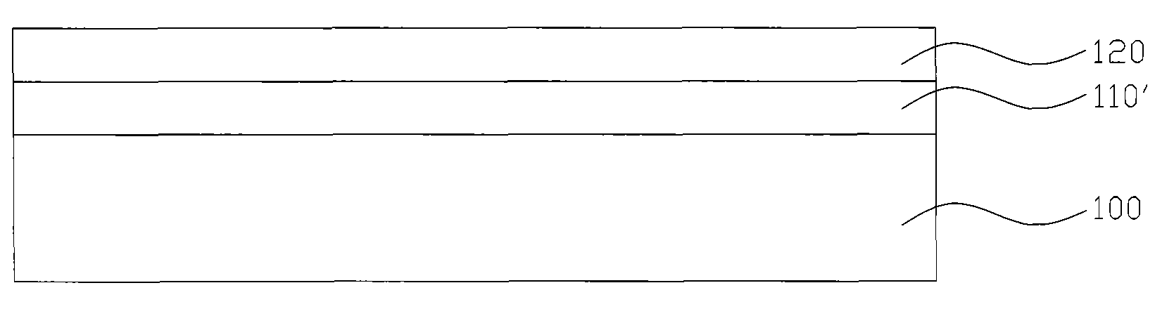
[0081] Figure 4 to Figure 8 It is a schematic diagram of the method for forming the pre-metal dielectric layer described in this embodiment. The pre-metal dielectric layer is a laminated dielectric layer composed of a first dielectric layer and a second dielectric layer on the first dielectric layer. Among them, the first dielectric layer adopts CVD process with good gap filling ability, especially for 65nm or below process, it is formed by HARP SACVD process; while the second dielectric layer adopts HDPCVD, PECVD or traditional SACVD with relatively high production capacity, etc. craft formation.

[0082] The reason why stacking dielectric layers are used to form the pre-metal dielectric layer is because as the feature size decreases, the aspect ratio of the gap becomes larger and larger. HDPCVD, PECVD or traditional SACVD processes can no longer satisfy the filling aspect ratio greater than The 7:1 gap requirement, and the HARP SACVD process has excellent gap filling abil...

Embodiment 2

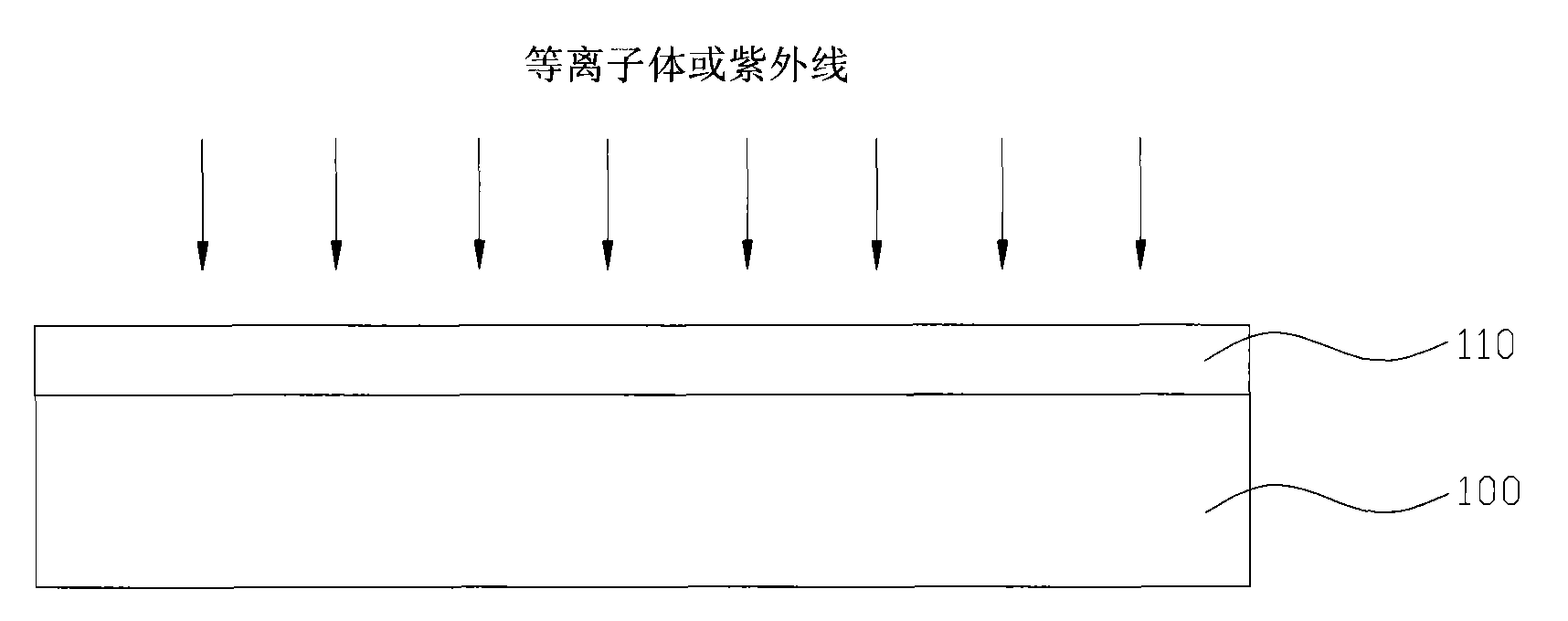
[0099] The difference between the method for forming the pre-metal dielectric layer in this embodiment and the first embodiment is that the first dielectric layer is dehumidified by ultraviolet irradiation in an oxygen-containing atmosphere.

[0100] Such as Figure 11 As shown, a gate 401 and a side wall 403 surrounding the gate are formed on a semiconductor substrate 400 with an active region through a front-end process, and a barrier layer 405 is formed, and then a first HARP SACVD process is used on the barrier layer 405. Dielectric layer 410 . The processes and materials used for the above-mentioned gate 401 , sidewall 403 , barrier layer 405 and first dielectric layer 410 are the same as those in Embodiment 1, and will not be repeated here.

[0101] Before forming the second dielectric layer, the first dielectric layer 410 is irradiated with ultraviolet rays in an oxygen-containing atmosphere to perform dehumidification treatment. The oxygen-containing atmosphere inclu...


PUM


Abstract

The invention discloses a laminated dielectric layer forming method, comprising the following steps: providing a substrate with a semiconductor structure; forming a first dielectric layer on the structure; adopting damp-removing process to the first dielectric layer; forming a second dielectric layer on the first dielectric layer which goes through damp-removing process. The invention also discloses a metal foredielectric layer forming method. With the methods of the invention adopted, the stress of the first dielectric layer in the laminated dielectric layer can be restored and maintained, therefore, the expected stress condition of the dielectric layer is increased.

Description

technical field [0001] The invention relates to the technical field of semiconductor manufacturing, in particular to a method for forming a laminated dielectric layer and a method for forming a pre-metal dielectric layer. Background technique [0002] With the increasing demand for high integration and high performance of ultra-large-scale integrated circuits, semiconductor technology is developing towards a technology node with a feature size of 65nm or even smaller. When the device size is continuously reduced proportionally, the interstitial ability of thin film deposition is also required ( Gap-fill ability) has been further improved. [0003] In the semiconductor manufacturing process, a dielectric layer is usually deposited on the substrate manufactured by the front-end process. In order to obtain reliable device performance, the dielectric layer needs to separate the gaps of the semiconductor structure on the substrate (including gate intervals, shallow trench isolati...

Claims


Application Information

Patent Timeline
IPC IPC(8): H01L21/31H01L21/3105H01L21/768
Inventor 徐强郑春生
Owner SEMICONDUCTOR MANUFACTURING INTERNATIONAL (BEIJING) CORP
Why Eureka
Try Eureka