Method for manufacturing capacitor of semiconductor device

A technology of electrodes and dielectric layers, which is applied in the field of semiconductor device capacitor manufacturing to achieve the effects of avoiding short circuits, improving product yield, excellent process reliability and productivity

Inactive Publication Date: 2009-12-09
DONGBU HITEK CO LTD
View PDF0 Cites 4 Cited by
  • Summary
  • Abstract
  • Description
  • Claims
  • Application Information

AI Technical Summary

Problems solved by technology

However, since the operating voltage (V) decreases with the increasing integration of memory devices, the capacitance (C) must be increased to obtain a sufficient amount of charge

Method used


Image

  • Method for manufacturing capacitor of semiconductor device
  • Method for manufacturing capacitor of semiconductor device
  • Method for manufacturing capacitor of semiconductor device

Examples


Embodiment Construction

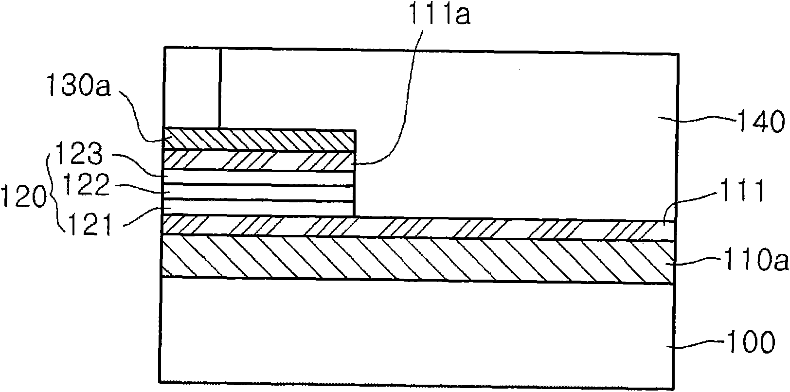
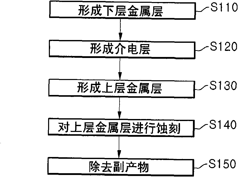
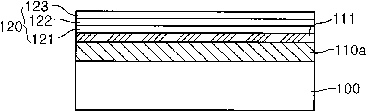
[0018] Hereinafter, a method of manufacturing a semiconductor device capacitor of the present invention will be described with reference to the accompanying drawings. figure 1 It is a sectional view of the semiconductor device capacitor of the present invention. refer to figure 1 A barrier metal layer (barrier metal layer) 111 is laminated on the lower electrode 110 a formed on the substrate, and a dielectric layer pattern may be formed on the barrier metal layer 111 . An upper barrier metal layer 111a may be laminated on the dielectric layer pattern, and an upper electrode 130a may be formed on the upper barrier metal layer 111a.

[0019] The lower electrode 110a and the upper electrode 130a may be a copper metal layer. When the lower electrode 110a and the upper electrode 130a are formed as copper metal layers, a damascene process may be used. According to the damascene process, the insulating layer is partially etched by a photoetching process to form a trench, and a cop...


PUM

PropertyMeasurementUnit
band gapaaaaaaaaaa

Abstract

A method for manufacturing a capacitor of a semiconductor device includes forming a lower metal layer over a substrate, forming a dielectric layer over the lower metal layer, forming an upper metal layer over the dielectric layer, forming an upper electrode and a dielectric layer pattern by performing a reactive ion etching process with respect to the upper metal layer using the dielectric layer as an etch stop layer, and exposing a top surface of the lower metal layer, and performing a chemical down-stream etch (CDE) process to remove a by-product of a sidewall of the upper electrode.

Description

technical field [0001] The invention relates to a method for manufacturing a semiconductor device capacitor. Background technique [0002] Capacitors may be used to store predetermined data in memory devices such as dynamic random access memory (DRAM). The capacitor includes capacitor electrodes called storage nodes and plate nodes and a dielectric layer interposed between the capacitor electrodes. [0003] Recently, due to the increasing integration of semiconductor storage devices, the chip area of ​​the storage battery in the semiconductor storage device is reduced, and the operating voltage of the semiconductor storage device is reduced. Based on this, even in the case where the design area of ​​the capacitor is reduced, it is necessary for the capacitor, which is one of the components of the semiconductor memory device, to have a charge amount necessary for the operation of the semiconductor memory device. If the charge amount is insufficient, problems such as soft er...

Claims


Application Information

Patent Timeline
Patent Type & Authority Applications(China)
IPC IPC(8): H01L21/02H01L21/28C23F4/00
CPCH01L21/02071H01L28/75H01L21/0206H10B99/00H10B12/00
Inventor 梁泽承
Owner DONGBU HITEK CO LTD
Why Eureka
Try Eureka