Structure for encapsulating multichip LED

A technology of LED packaging and packaging structure, applied in the direction of semiconductor/solid-state device components, semiconductor devices, electrical components, etc., can solve problems such as LED damage, affecting reliability and life, and achieve expanded contact, increased working voltage, and anti-electricity high impact effect

Inactive Publication Date: 2009-12-30
刘红超
View PDF0 Cites 18 Cited by
  • Summary
  • Abstract
  • Description
  • Claims
  • Application Information

AI Technical Summary

Problems solved by technology

These instantaneous energy signals can emit tens of watts, which will cause damage to the LED and affect its reliability and lifespan.

Method used


Image

  • Structure for encapsulating multichip LED
  • Structure for encapsulating multichip LED
  • Structure for encapsulating multichip LED

Examples


Embodiment 1

[0035]Embodiment 1 Encapsulation of a single high-power LED chip.

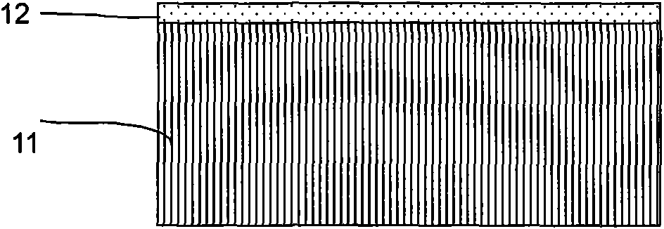
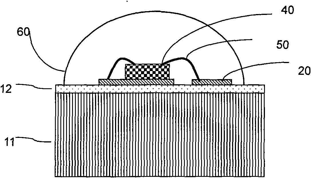
[0036] figure 1 is the structure of the substrate 10 . Its lower layer 11 is a metal with good heat dissipation, and the first choice is light in weight, high in thermal conductivity, and easy to process aluminum and becomes the first choice. The upper layer 12 is a film grown by sputtering, preferably AlN and SiC.

[0037] figure 2 , 3, 4, is a structure in which a single high-power LED chip 40 and a transient protection diode 30 are packaged together. The bracket 20 is prefabricated in a certain shape, and its material is preferably copper, on which tin is plated as required. The LED and the transient protection chip are bonded on the bracket 20 with an adhesive, such as silver paste. After baking and fixing, use a bonding machine to make connecting wires 50, mainly gold wires here, and weld the positive and negative electrodes of the chips 30 and 40 to the bracket 20 respectively. Evenly spread a thi...

Embodiment 2

[0038] Embodiment 2 Packaging of Multi-chip Parallel LEDs

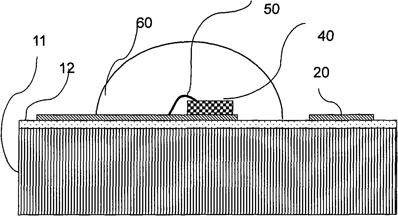
[0039] Using the same production method as in Embodiment 1, changing the shape of the support 20 can produce high-power LEDs formed by parallel connection of smaller power chips. Figure 5 A method of connecting 16 low-power LED chips 40 and a protection chip 30 in parallel to form a 1W power LED is shown. This method not only reduces the thermal resistance between different layers, but also increases the heat dissipation area of ​​the LED chip, so the resistance of the system is reduced by about 30% compared with the conventional packaging method.

Embodiment 3

[0040] Embodiment 3 Packaging of multi-chip series-parallel LEDs

[0041] Figure 6 16 LED chips 40 and one protection chip 30 are packaged in series and parallel. The feature of this packaging method is that it can change the driving voltage of the finished LED product and improve the energy replacement efficiency of the power supply. Although LED is a light source with high energy efficiency, its final power conversion efficiency is also affected by power conversion efficiency. As we all know, LED is a low-voltage current-driven device. In order to make it work stably and reliably, it is necessary to change the power supply voltage, such as replacing AC with DC, and replacing high-voltage DC with low-voltage DC. Constant current, and these conversions will lose some energy. If the working conditions of the LED can be made as close as possible to the voltage conditions of the power supply, this part of energy loss can be reduced and the overall energy conversion efficiency...


PUM


Abstract

The invention provides an LED encapsulating structure which can radiate in high efficiency and has transient voltage protection and high energy efficiency. The LED encapsulating structure mainly comprises a substrate, a bracket, LED chips, a transient protection chip, a connecting wire and an encapsulating colloid. The substrate has a double-layer structure; the lower layer of the substrate is made of a metal material with good radiation; and the upper layer is a film with high thermal conductivity and electrical insulation. The bracket is a good heat and electricity conductor; and the shape of the bracket can be adjusted according to the requirements, such as the number of the chips, a connecting method and the like. The transient voltage protection chip and the LED chip are arranged on the bracket; and the bracket is directly arranged on the substrate. The positions of the chip and the connecting wire needing protection are encapsulated by the colloid; and the exposed bracket part forms a connecting part of an external power supply. A plurality of the LED chips can be connected in a parallel mode or a serial-parallel mode so as to be favorable for improving the conversion efficiency of the power supply; and a plurality of the LED chips can also form multi-circuit connection to independently control the LEDs of each circuit. A plurality of LED light sources can be flexibly obtained according to the method.

Description

technical field [0001] The invention relates to semiconductor lighting technology, in particular to a packaging and manufacturing method for light-emitting diodes as the main device, especially a packaging method for improving heat dissipation and its ability to resist transient voltage impacts, and is suitable for light-emitting diodes and similar semiconductor devices. technical background [0002] LED uses a semiconductor PN junction as a light source, and the energy of its forbidden band corresponds to a certain wavelength of light, that is, after electrons and holes are matched, the excess energy is radiated in the form of photons. LED has become the fourth generation light source because of its energy saving, environmental protection, small size, flexible use, high reliability and long life. At present, it is widely used in LCD screen backlight, traffic signal lights, exterior wall decoration, medical treatment, lighting, large-screen display, car lights, etc. Accordi...

Claims


Application Information

Patent Timeline
Patent Type & Authority Applications(China)
IPC IPC(8): H01L25/16H01L23/36H01L23/367H01L23/373H01L21/50H01L33/00
CPCH01L2224/48237H01L2224/48137H01L2224/48091H01L2224/49113H01L2924/00014
Inventor 刘红超
Owner 刘红超
Why Eureka
Try Eureka