

Technique for processing silicon chip
A processing technology and technology of silicon wafers, applied in the direction of electrical components, semiconductor/solid-state device manufacturing, circuits, etc., can solve problems such as increasing product costs, achieve the effects of increasing yield, reducing removal amount, and ensuring processing accuracy
- Summary
- Abstract
- Description
- Claims
- Application Information
AI Technical Summary
Problems solved by technology
Method used
Image

Examples
Embodiment 1
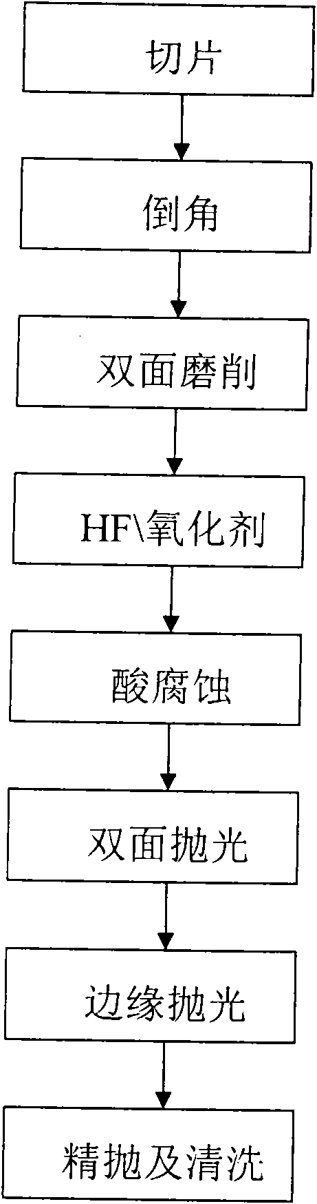
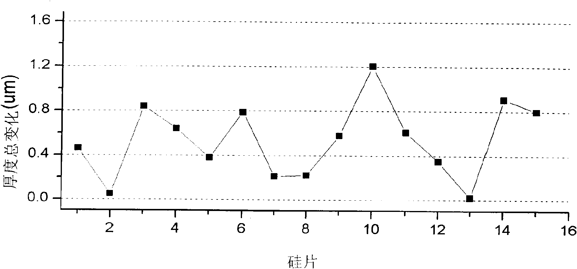
[0031] Use the P (100) produced by the Czochralski method, 15 pieces of 12-inch double-sided grinding discs with a resistivity of 1-3Ωcm, and use the HF tank to add H on a conventional cleaning machine 2 o 2 Or the mixture of hydrofluoric acid and O3, usually the concentration of hydrofluoric acid is 49%, H 2 o 2 The concentration is 30% (their usage ratio is 1:0.5) to rinse the silicon wafer to remove the microscopic raised parts on the surface, and then perform etching on an acid etching machine, and the etching removal amount is 15 microns. AFS3220 geometric parameter tester was used to measure the geometric parameters of the silicon wafer before and after treatment, so as to obtain the change of GBIR before and after acid corrosion. The change of GBIR (total thickness) before and after corrosion is less than 0.9 microns, and the change of GBIR of each piece is as follows: image 3 shown. It can be seen from the figure that the change of GBIR is small, which shows that ...
Embodiment 2
[0033] Take the above 15 silicon wafers etched by acid, and use the method of the present invention to perform double-sided polishing on a Speedfam20B polishing machine, and the polishing removal amount is 15 microns. Then wash it with a washing machine and dry it with a spin dryer. See GBIR after polishing. Figure 4 . It can be seen from the figure that after the present invention, the total removal amount after grinding is only 30 microns, but the precision is higher.
Embodiment 3
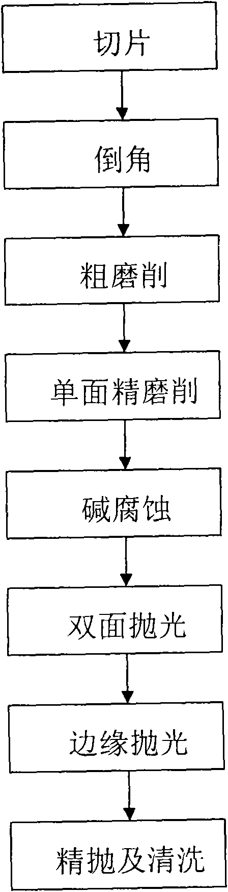
[0035] Get above 15 double-sided grinding sheets and process with the existing technology at present. In order to remove the disc marks on the surface, use a single-side grinder for fine grinding, removing 10 microns per side (20 microns in total). Then the grinding sheet is corroded by alkali corrosion to remove the damage on the surface, and the removal amount is 15 microns. Finally, double-sided polishing is performed with a removal volume of 15 microns. After processing by the current processing technology, the removal amount is 50 microns.
PUM
 Abstract
Description
Claims
Application Information