Method for selectively removing TaN metal gate electrode layer

A metal gate and electrode layer technology, applied in the field of selective removal of metal gate electrode layer, selective removal of TaN metal gate electrode layer, can solve the problems of low selection ratio, inapplicable selective removal of TaN metal gate electrode layer, etc.

Active Publication Date: 2010-02-24
INST OF MICROELECTRONICS CHINESE ACAD OF SCI
View PDF0 Cites 11 Cited by
  • Summary
  • Abstract
  • Description
  • Claims
  • Application Information

AI Technical Summary

Problems solved by technology

[0004] According to the present invention, after selectively removing the first TaN metal gate electrode layer by wet etching, a solution containing HF is needed to remove the TEOS hard mask, but the solution containing HF has a very low selectivity for high-K gate dielectric layers such as HfSiON Low, so that there is a compatibility problem between the TEOS hard mask and the HfSiON high-K gate dielectric layer, and it is not suitable for realizing the selective removal of the TaN metal gate electrode layer on the HfSiON high-K gate dielectric layer. Provide a selective removal TaN metal gate electrode layer method

Method used


Image

  • Method for selectively removing TaN metal gate electrode layer
  • Method for selectively removing TaN metal gate electrode layer
  • Method for selectively removing TaN metal gate electrode layer

Examples


Embodiment Construction

[0030] The principles and features of the present invention are described below in conjunction with the accompanying drawings, and the examples given are only used to explain the present invention, and are not intended to limit the scope of the present invention.

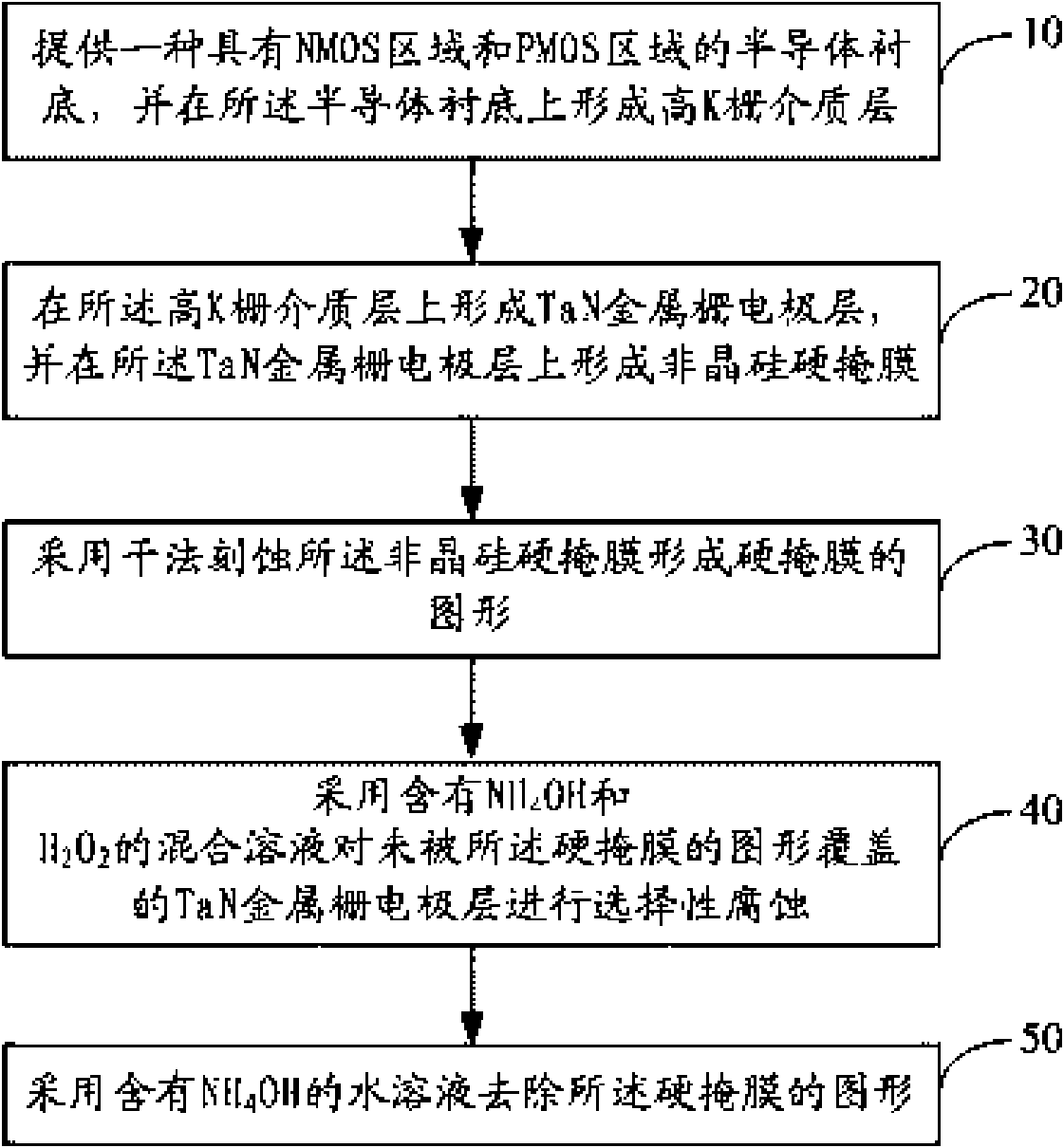
[0031] figure 1 It is a flowchart of a method for selectively removing a TaN metal gate electrode layer according to an embodiment of the present invention. Such as figure 1 As shown, the method includes the following steps:

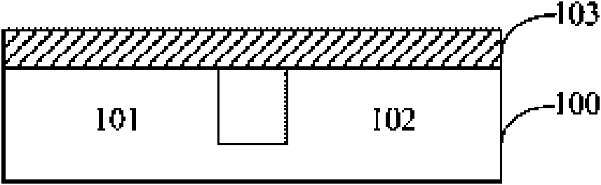
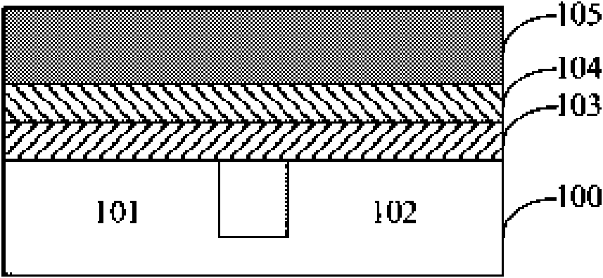
[0032] Step 10: providing a semiconductor substrate 100 having an NMOS region 101 and a PMOS region 102 , and forming a high-K gate dielectric layer 103 on the semiconductor substrate 100 .

[0033] The high-K gate dielectric layer 103 is made of HfO 2 , HfON, HfAlO, HfAlON, HfTaO, HfTaON, HfSiO, HfSiON, HfZrO, HfZrON, HfLaO or HfLaON, and its thickness is 2 nm to 4 nm. The high-K gate dielectric layer 103 can be formed by conventional deposition methods, such as physical vapor deposition,...


PUM

PropertyMeasurementUnit
thicknessaaaaaaaaaa
thicknessaaaaaaaaaa
thicknessaaaaaaaaaa

Abstract

The invention relates to a method for selectively removing a TaN metal gate electrode layer, belonging to the technical field of integrated circuit manufacture. The method comprises the following steps: forming a high K gate dielectric layer on a semiconductor substrate; forming a TaN metal gate electrode layer on the high K gate dielectric layer and forming an amorphous silicon hard mask on the TaN metal gate electrode layer; etching the amorphous silicon hard mask by adopting a dry method to form hard mask patterns; selectively corroding the TaN metal gate electrode layer uncovered by the hard mask patterns by adopting wet method corrosion; and removing the hard mask patterns by adopting the wet method corrosion. The method uses amorphous silicon as the hard mask and removes the TaN metal gate electrode layer with a high selection ratio by adopting the wet method corrosion of the TaN metal gate electrode layer. In addition, the method has high selection ratios to the TaN metal gate electrode layer and the high K gate dielectric layer when adopting a wet method corrosion solution to remove residential amorphous silicon hard mask and does not has compatibility problem.

Description

technical field [0001] The invention relates to a method for selectively removing a metal gate electrode layer, in particular to a method for selectively removing a TaN metal gate electrode layer, and belongs to the technical field of integrated circuit manufacturing. Background technique [0002] As the feature size of semiconductor devices enters the 45nm technology node, high K (dielectric constant) / metal gate materials are used instead of traditional SiO 2 / poly (polysilicon) structure has become an inevitable choice. TaN metal gate material has become a nanoscale CMOS (complementary type) due to its good thermal stability, chemical stability, controllable work function, and good adhesion to Hf-based high-permittivity gate dielectrics. A strong candidate for NMOSFET (N-type metal-oxide-semiconductor field effect transistor) metal gate materials in metal-oxide-semiconductor field-effect transistor) devices. In order to realize the different requirements of N / PMOSFET on ...

Claims


Application Information

Patent Timeline
Patent Type & Authority Applications(China)
IPC IPC(8): H01L21/28H01L21/8238
Inventor 李永亮徐秋霞
Owner INST OF MICROELECTRONICS CHINESE ACAD OF SCI
Why Eureka
Try Eureka