Method for preparing light absorption layer of CuInSe2 (CIS) based thin film solar cell

A technology for solar cells and light-absorbing layers, applied to coatings, circuits, electrical components, etc., can solve problems such as loss, complex equipment structure, and many defects in the absorption layer, and achieve high production efficiency and simple equipment structure

Inactive Publication Date: 2010-03-03
INST OF ELECTRICAL ENG CHINESE ACAD OF SCI
View PDF0 Cites 18 Cited by
  • Summary
  • Abstract
  • Description
  • Claims
  • Application Information

AI Technical Summary

Problems solved by technology

The difficulty of preparing a large-size absorbing layer by the post-selenization method of the metal film lies in: (1) Because Ga has a large diffusion coefficient and is easy to react with the Mo electrode, it is difficult for Ga to enter the lattice position to form effective doping; (2) Improper control of the selenium atmosphere may cause the loss of Cu and In during the selenization process; (3) During the selenization process, selenium reacts with the metal preset film, and the large vo

Method used


Image

  • Method for preparing light absorption layer of CuInSe2 (CIS) based thin film solar cell
  • Method for preparing light absorption layer of CuInSe2 (CIS) based thin film solar cell
  • Method for preparing light absorption layer of CuInSe2 (CIS) based thin film solar cell

Examples


Example Embodiment

[0024] Example 1

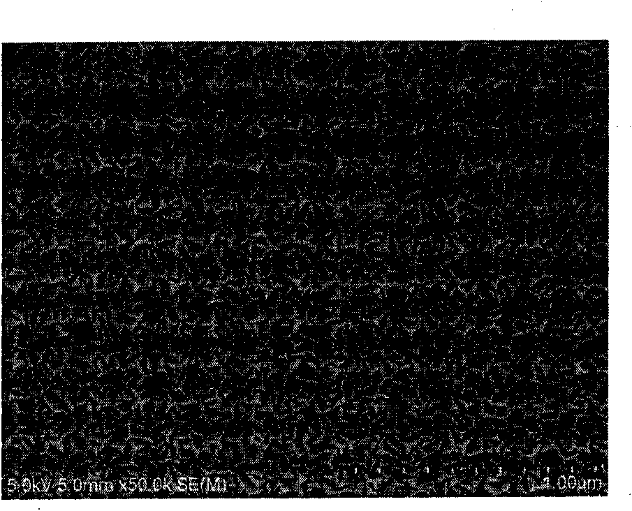
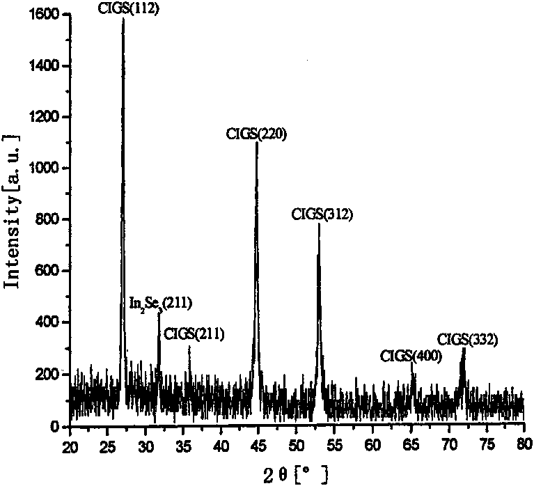
[0025] The sputtering target used is CuIn with a purity of 99.99% 0.7 Ga 0.3 Se 2.2 Ceramic target, the size is φ70×3mm, (CuIn 0.7 Ga 0.3 Se 2.2 The ceramic target is commercially available and produced by Beijing Changhao Youyan New Material Technology Development Co., Ltd. CuIn is used in the following examples 0.7 Ga 0.3 Se 2.2 The ceramic target is the same) The X-ray diffraction pattern of the ceramic target used is as follows image 3 Shown. The preparation steps of this embodiment are as follows:

[0026] (1) Cut the soda glass into a 10×10mm substrate, first put it in deionized water for ultrasonic cleaning for 5 minutes to remove the debris generated during the cutting process, and then put it in acetone for ultrasonic cleaning for 15 minutes to remove the oil on the surface of the substrate. Then put the substrate in alcohol for ultrasonic cleaning for 2 minutes, and finally dry the substrate for use;

[0027] (2) Put the cleaned soda glass substrate int...

Example Embodiment

[0032] Example 2

[0033] The sputtering target used is CuIn with a purity of 99.99% 0.7 Ga 0.3 Se 2.2 Ceramic target, the size is φ70×3mm, the preparation steps are as follows:

[0034] (1) Cut the soda glass into a 10×10mm substrate, first put it in deionized water for ultrasonic cleaning for 5 minutes to remove the debris generated during the cutting process, and then put it in acetone for ultrasonic cleaning for 15 minutes to remove the oil on the surface of the substrate. Then put the substrate in alcohol for ultrasonic cleaning for 2 minutes, and finally dry the substrate for use;

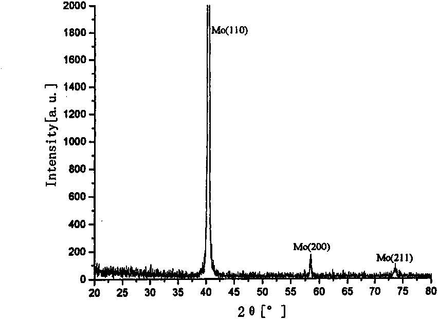
[0035] (2) Put the cleaned soda glass substrate into the cavity of the magnetron sputtering equipment, install a Mo target in the cavity (the purity of the Mo target is 99.99%), the target base distance is 50mm, and then the cavity The body is evacuated to a vacuum degree of less than 3.0×10 -3 Pa, then argon gas was introduced, the pressure was adjusted to 1 Pa, sputtering started, and the sputter...

Example Embodiment

[0039] Example 3

[0040] The sputtering target used is CuIn with a purity of 99.99% 0.7 Ga 0.3 Se 2.2 Ceramic target, the size is φ70×3mm. The preparation steps are as follows:

[0041] (1) Cut the soda glass into a 10×10mm substrate, first put it in deionized water for ultrasonic cleaning for 5 minutes to remove the debris generated during the cutting process, and then put it in acetone for ultrasonic cleaning for 15 minutes to remove the oil on the surface of the substrate. Then put the substrate in alcohol for ultrasonic cleaning for 2 minutes, and finally dry the substrate for use;

[0042] (2) Put the cleaned soda glass substrate into the cavity of the magnetron sputtering equipment, install Mo target in the cavity (Mo target purity is 99.99%), the target base distance is 60mm, and then vacuum to vacuum Degree less than 3.0×10 -3 Pa, then argon gas was introduced, the pressure was adjusted to 1 Pa, sputtering started, and the sputtering power was slowly increased to 120W. Af...


PUM

PropertyMeasurementUnit
Thicknessaaaaaaaaaa
Resistivityaaaaaaaaaa
Thicknessaaaaaaaaaa

Abstract

The invention relates to a method for preparing a light absorption layer of CuInSe2(CIS) based thin film solar cell. The method includes the following steps: firstly, sputtering Mo electrodes requiredfor preparing the CIS radical thin film solar cell on a soda glass substrate; then sputtering on the Mo electrodes by taking CuIn0.7Ga0.3Se2.2 as target to obtain a CuIn0.7Ga0.3Se2.0 (CIGS) thin filmin deposited status; subsequently conducting heat treatment on the CIGS thin film in deposited status: filling argon in a vacuum cavity to 100Pa, heating up the CIGS thin film in deposited status atthe heating rate of 20-40 DEG C/min to 450-550 DEG C, preserving the heat for 15min, then reducing the temperature to 350 DEG C at the temperature reduction rate of 20-40 DEG C/min, cooling to the room temperature with a furnace and obtaining the light absorption layer of CuInSe2 radical thin film solar cell CIGS.

Description

technical field [0001] The invention relates to a method for preparing thin film solar cells, in particular to the preparation of CuInSe 2 A method for light-absorbing layer-based thin-film solar cells. Background technique [0002] copper indium selenide (CuInSe 2 , referred to as CIS)-based thin-film solar cells are the most representative photovoltaic devices in compound semiconductors. Because of its high conversion efficiency, low manufacturing cost and stable performance, it has become one of the research hotspots in the international photovoltaic industry, and it is likely to become the next generation of commercial thin-film solar cells. [0003] The light-absorbing layer is the core functional layer of CIS-based thin-film solar cells, and the quality of this layer directly affects the photoelectric conversion efficiency of the cell. The light absorption layer of CIS-based thin film solar cells mainly includes CuIn x (Ga, Al) 1-x Se y (S, Te) 2-y (x=0~1, y=0~2...

Claims


Application Information

Patent Timeline
IPC IPC(8): H01L31/18H01L31/0224H01L31/0216C23C14/34C23C14/18C23C14/35C23C14/06
CPCY02P70/50
Inventor 古宏伟丁发柱
Owner INST OF ELECTRICAL ENG CHINESE ACAD OF SCI
Why Eureka
Try Eureka