

Film forming method and film forming apparatus
A film-forming device and thin-film technology, which is applied in the direction of gaseous chemical plating, coating, electrical components, etc., can solve the problems of long time, production capacity decline, etc., and achieve the effect of improving processing capacity, improving adhesion, and suppressing the generation of particles
- Summary
- Abstract
- Description
- Claims
- Application Information
AI Technical Summary
Problems solved by technology
Method used
Image

Examples
Embodiment Construction
[0049] Next, a preferred embodiment of the film forming method and film forming apparatus of the present invention will be described with reference to the drawings.
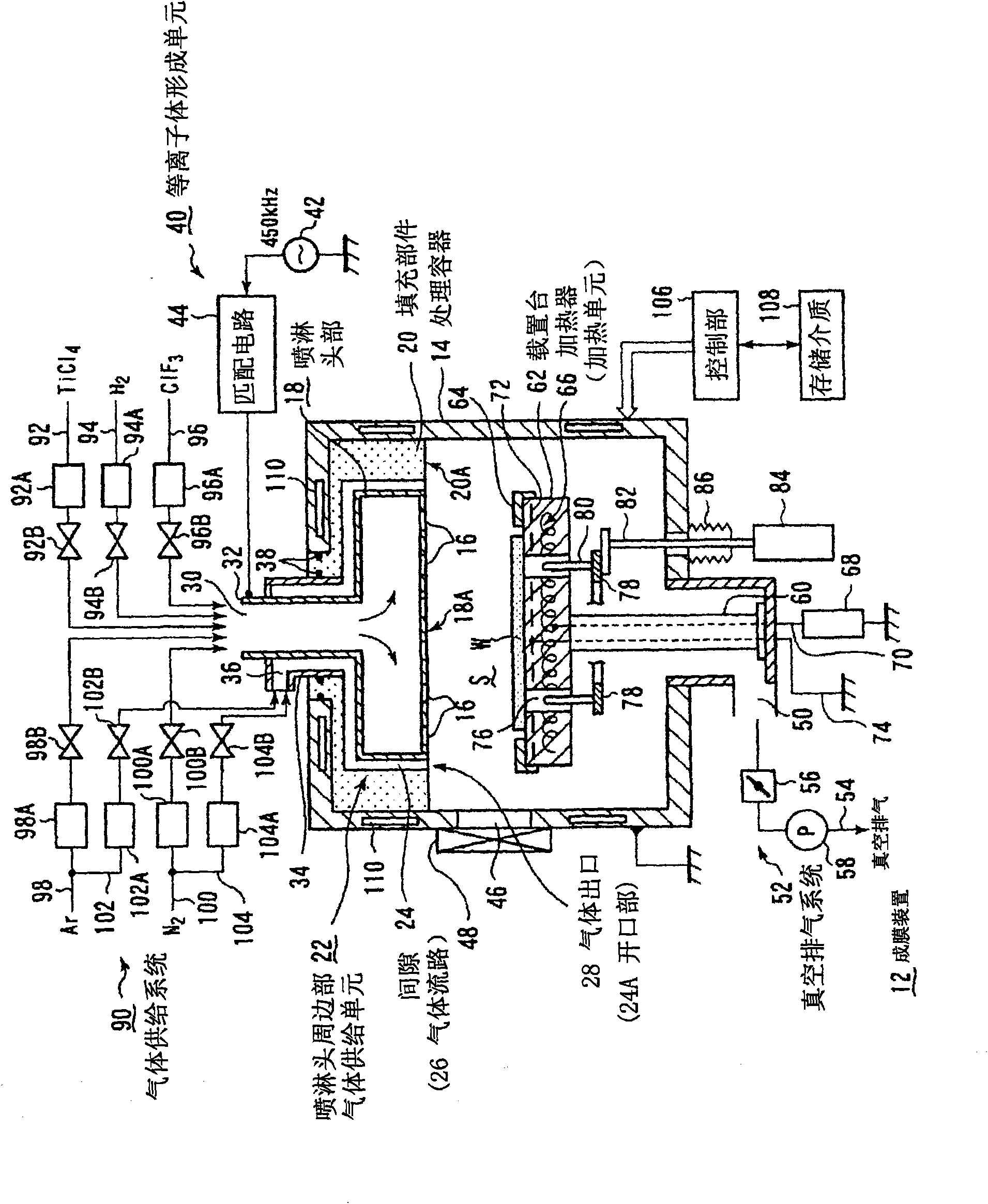
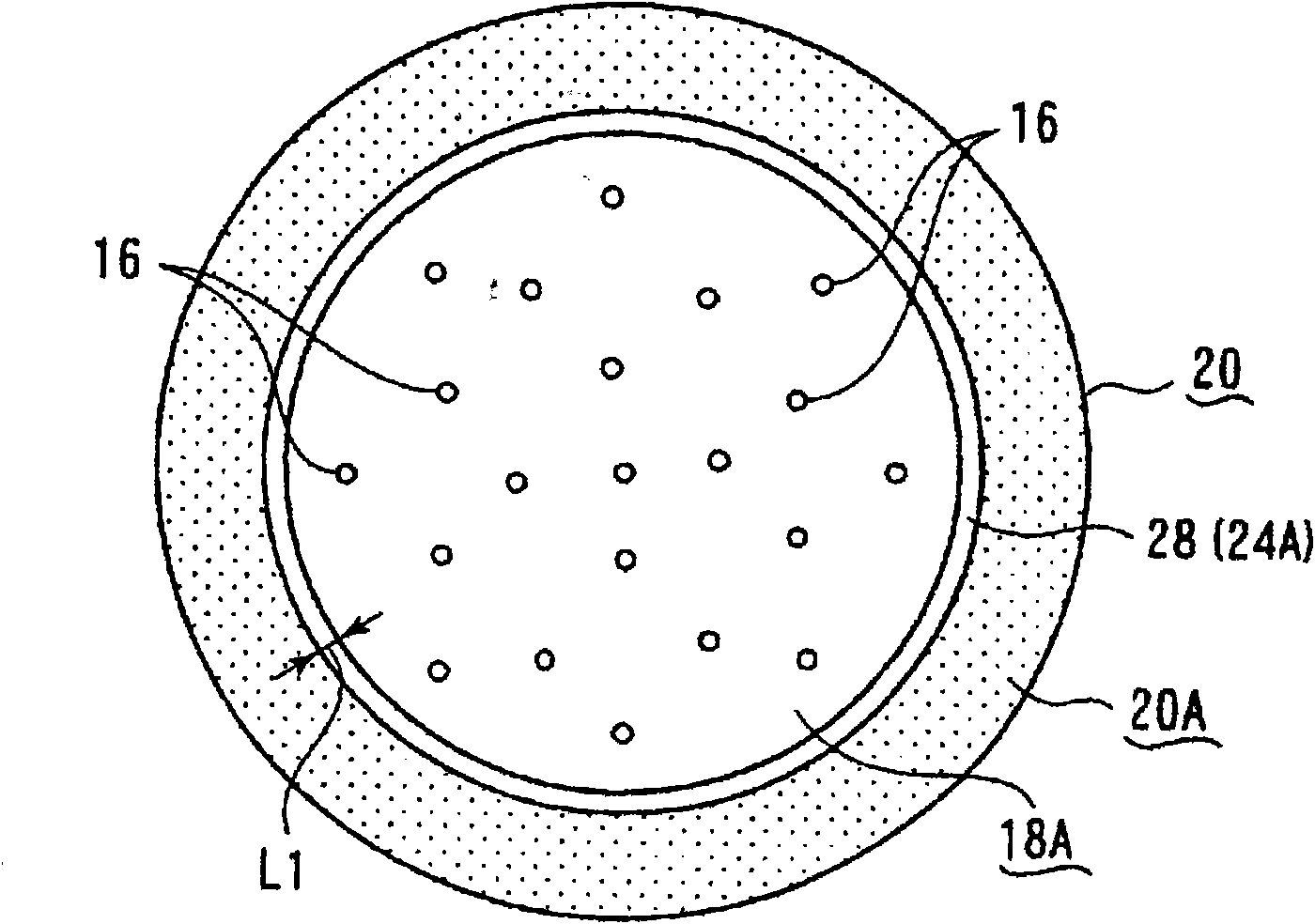
[0050] figure 1 is a cross-sectional structural view showing an example of a film forming apparatus for carrying out the film forming method of the present invention. figure 2 It is a plan view showing the gas injection surface side of the shower head. Here, a case where a titanium film (Ti film) is formed as a thin film by plasma CVD will be described as an example.
[0051] As shown in the figure, the film forming apparatus 12 has a cylindrical processing container 14 made of, for example, aluminum or an aluminum alloy, and the processing container 14 is grounded. A shower head 18 is provided on the top of the processing container 14, and the shower head 18 has a plurality of gas ejection ports 16 on the lower surface as a gas introduction unit (refer to figure 2 ), so that various necessary gases can be ...
PUM
| Property | Measurement | Unit |
|---|---|---|
| thickness | aaaaa | aaaaa |
Abstract
Description
Claims
Application Information