Check patentability & draft patents in minutes with Patsnap Eureka AI!

LDMOS transistor structure and preparation method

A transistor and high-voltage technology, applied in the field of LDMOS transistor preparation, can solve the problems of increasing device area and cost, and achieve the effects of small product area, cost reduction, and design size reduction

Active Publication Date: 2011-08-24
SHANGHAI HUAHONG GRACE SEMICON MFG CORP
View PDF0 Cites 0 Cited by
  • Summary
  • Abstract
  • Description
  • Claims
  • Application Information

AI Technical Summary

Problems solved by technology

The most direct method is to increase the design length of the high withstand voltage shallowly doped region. However, it is obvious that the problem brought about by this is that the device area increases and the cost increases greatly, which is the least desirable

Method used


Image

  • LDMOS transistor structure and preparation method
  • LDMOS transistor structure and preparation method
  • LDMOS transistor structure and preparation method

Examples


Embodiment Construction

[0020] The LDMOS transistor structure of the present invention, starting from the electrical point of view, applies an electric field in the direction perpendicular to the level drop, so that the level drop line B has to turn under the action of the transverse electric field, thereby also achieving the purpose of increasing the level drop electric field.

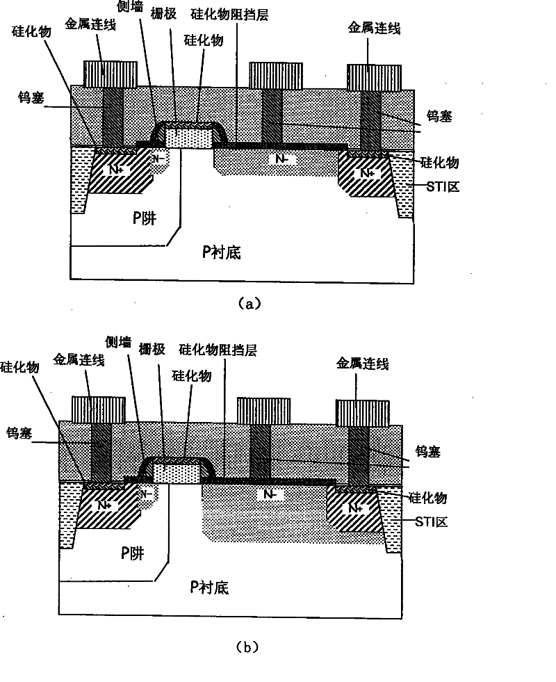
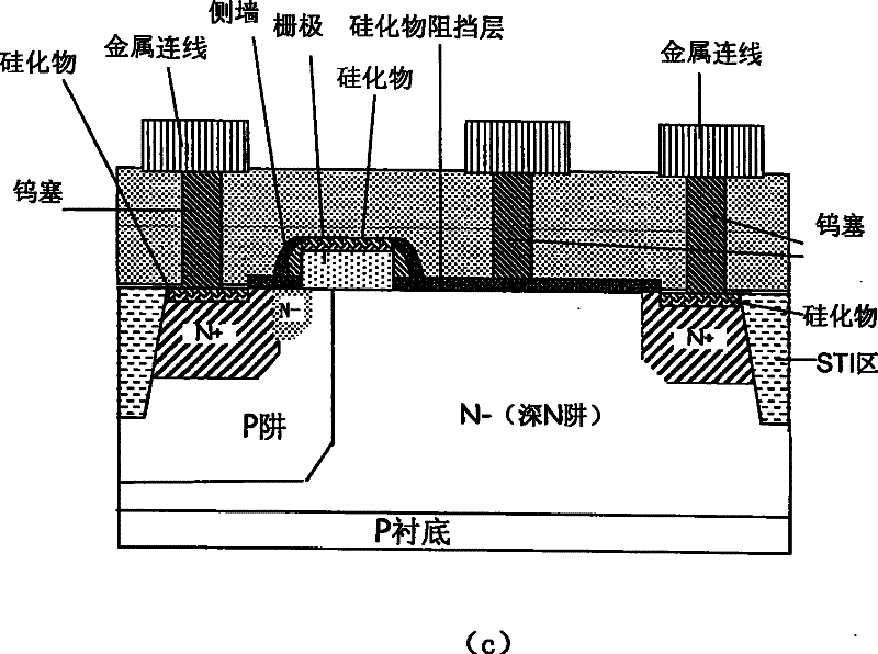
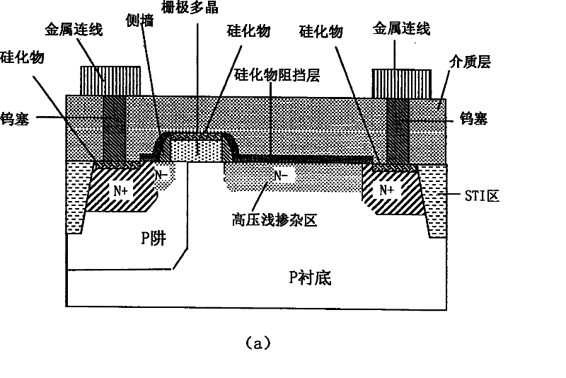
[0021] Such as Figure 7 (a) and Figure 7 As shown in (b), several contact holes or strip-shaped contact trenches are formed in the high-voltage shallow doped region (also called the withstand voltage region) of the traditional LDMOS device, and then the contact holes or contact trenches are filled with tungsten, and then Metal wiring is formed thereafter. The LDMOS transistor structure of the present invention includes a source heavily doped region, a source lightly doped region, a gate and gate sidewalls, a drain heavily doped region, and a silicon region on the side of the gate close to the drain to the drain. There is...


PUM


Abstract

The invention discloses an LDMOS transistor structure, which comprises a high-pressure shallow doped area between a lower silicon area at one side of a grid electrode close to a drain electrode and a heavily doped area of the drain electrode, wherein a silicide barrier layer and a dielectric layer are covered on the surface of the high-pressure shallow doped area, and the LDMOS transistor also comprises a contact hole or a contact groove which is filled with metal and is positioned on the silicide barrier layer on the surface of the high-pressure shallow doped area, and a metal connecting wire on the contact hole or the contact groove. The floating contact hole formed on the high-pressure shallow doped area of the LDMOS transistor structure enables a potential drop line to be bent when anLDMOS device works so as to improve the pressure resistance of the device. The invention also discloses a preparation method for the LDMOS transistor.

Description

technical field [0001] The invention relates to an LDMOS transistor structure. The invention also relates to the preparation method of the LDMOS transistor. Background technique [0002] With the development of semiconductor technology, the application of semiconductors has appeared in all walks of life, which has further requirements for semiconductors. Among them, high-voltage (working voltage greater than 15V) requires semiconductors to withstand working voltages exceeding the normal working environment. In such occasions, LDMOS (Laterally Diffused Metal Oxide Semiconductor Transistor) is a commonly used high-voltage MOS transistor structure. Common There are several structures, such as figure 1 (a), (b) and (c) are cross-sectional schematic diagrams of commonly used structures. by figure 1 (a) Donor LDMOS (hereinafter referred to as LDNMOS) as an example, such as figure 2 (a) Schematic details of the section and figure 2 As shown in the design layout of (b), in o...

Claims


Application Information

Patent Timeline
Patent Type & Authority Patents(China)
IPC IPC(8): H01L29/78H01L21/336
Inventor 陈俭
Owner SHANGHAI HUAHONG GRACE SEMICON MFG CORP
Features
  • R&D
  • Intellectual Property
  • Life Sciences
  • Materials
  • Tech Scout
  • Unparalleled Data Quality
  • Higher Quality Content
  • 60% Fewer Hallucinations
Learn More