Piezoelectric transformer
A piezoelectric transformer and piezoelectric substrate technology, applied in the field of piezoelectric transformers, can solve problems such as hysteresis loss, increased eddy current loss, and electromagnetic noise
- Summary
- Abstract
- Description
- Claims
- Application Information
AI Technical Summary
Problems solved by technology
Method used
Image
Examples
Embodiment 1
[0165] 【0067】
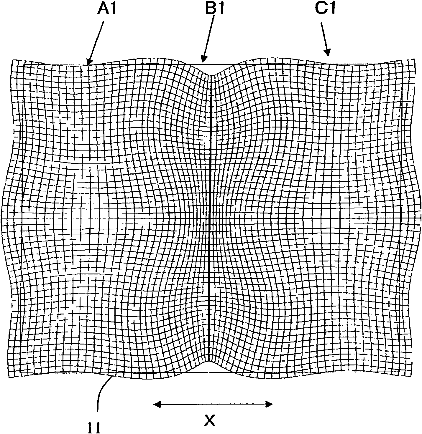
[0166] Computer simulations using the finite element method were performed for the piezoelectric transformer of the present invention.
[0167] 【0068】
[0168] Pb(Ti, Zr)O is assumed as the material of the piezoelectric transformer 3 Piezoelectric material, in the simulation, set the piezoelectric constant d 31 =-125pC / m, relative permittivity εr=1420, Qm=1000, and calculated.
[0169] 【0069】
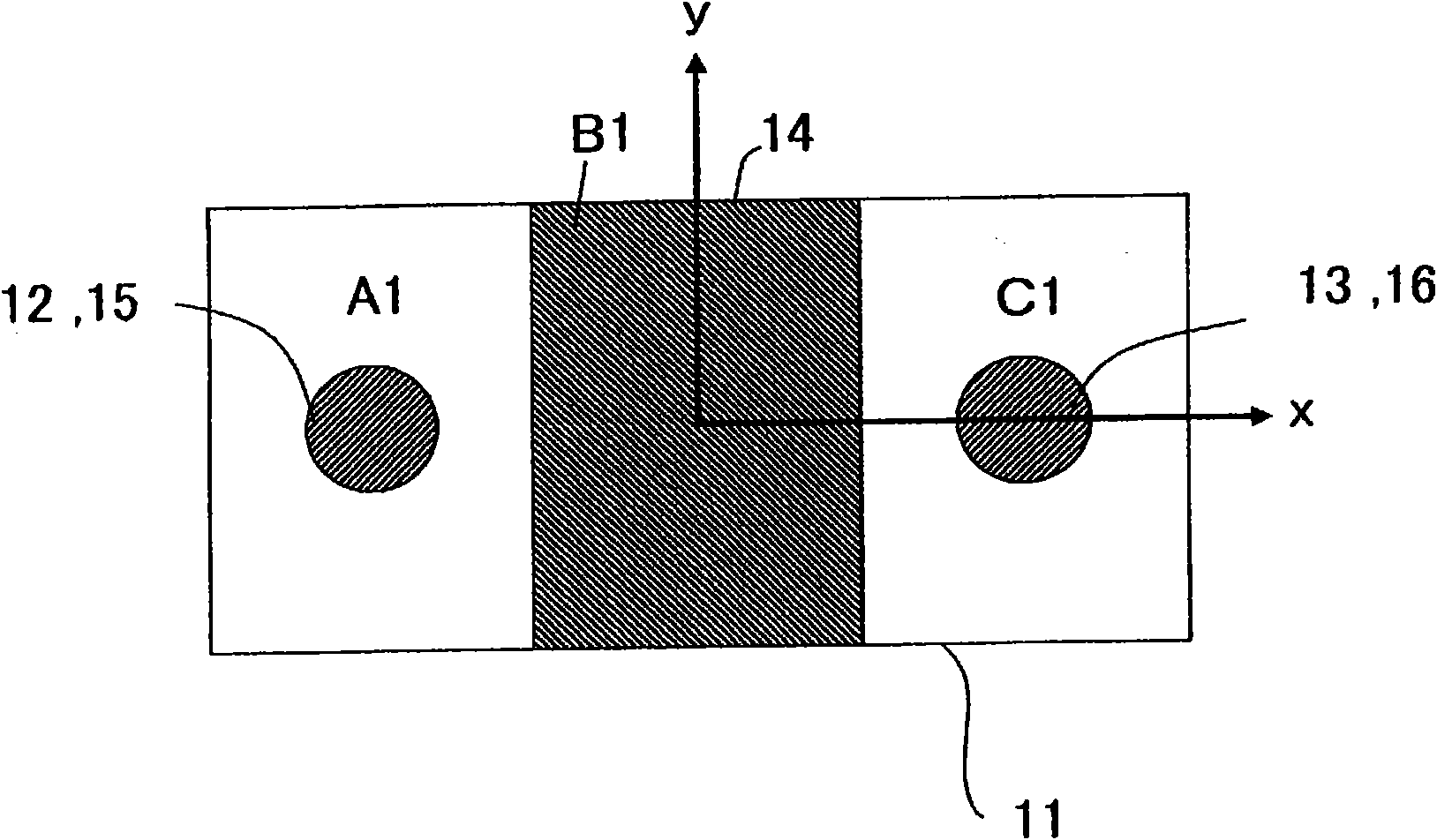
[0170] exist Figure 8 A mesh segmentation diagram of the finite element model used in the simulation is shown in . In the simulation, consider the symmetry of the piezoelectric transformer, as figure 2 As shown, the upper right part of the same figure is simulated using a 1 / 4 symmetric model. exist Figure 8 Among them, symbol 42 represents a 1 / 4 symmetry plane.
[0171] 【0070】
[0172] The dimensions of the piezoelectric transformer were assumed to be length L = 31.5 mm, width W = 26.0 mm, and thickness T of the piezoelectric substrate = 2.1 mm. In addition...
Embodiment 2
[0184] 【0076】
[0185] If the electrode area is reduced all the way to about 5% as in S1, regardless of the choice of deformation S XX A drop in efficiency can be confirmed in a large area. In particular, it can be seen that the peak of efficiency at frequencies lower than 170 kHz becomes smaller. Due to the impedance matching of the input circuit and the limitation of the driving IC, etc., in the case of actually having to use it in an electrode such as S1, although it is desirable to use it at a frequency near 175kHz, it is due to the spuriousness caused by the unwanted vibration mode near 170kHz. , so the usable frequency band is narrowed.
[0186] 【0077】
[0187] Therefore, as shown in FIG. 13 , a rectangular notch is formed in the peripheral portion of the piezoelectric transformer to try to control the parasitic. As shown in FIG. 13, if four notches are formed in the peripheral portion of the piezoelectric substrate, the spurious caused by unwanted vibration can be s...
PUM
 Abstract
Description
Claims
Application Information


