Grooved gate IGBT with P-type floating layer

A floating layer and trench gate technology, applied in electrical components, electric solid devices, circuits, etc., can solve the problem of reduced short-circuit capability of insulated gate bipolar transistors, insufficient withstand voltage of insulated gate bipolar transistors, and increased saturation current. Density and other issues, to achieve the effect of improving the short-circuit safe working capacity, improving the short-circuit safe working area, and reducing the saturation current density

Inactive Publication Date: 2010-04-14
UNIV OF ELECTRONICS SCI & TECH OF CHINA
View PDF0 Cites 13 Cited by
  • Summary
  • Abstract
  • Description
  • Claims
  • Application Information

AI Technical Summary

Problems solved by technology

But at the same time, the increased saturation current density reduces the short-circuit capability of the IGBT controlled by the accumulation layer, and the breakdown voltage depends on the design size, making the IGBT controlled by the accumulation layer Insufficient pressure resistance

Method used


Image

  • Grooved gate IGBT with P-type floating layer
  • Grooved gate IGBT with P-type floating layer
  • Grooved gate IGBT with P-type floating layer

Examples


Embodiment Construction

[0034] By adopting the novel slot gate IGBT structure with floating P-type layer of the present invention, low turn-on voltage drop, large forward bias safe operating area (FBSOA) and short circuit safe operating area (SCSOA), low leakage current, and energy The breakdown voltage is further improved, the manufacture is simple, and the design margin is large. With the development of semiconductor technology, more low-voltage drop and high-reliability power devices can be produced by adopting the invention.

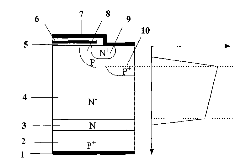
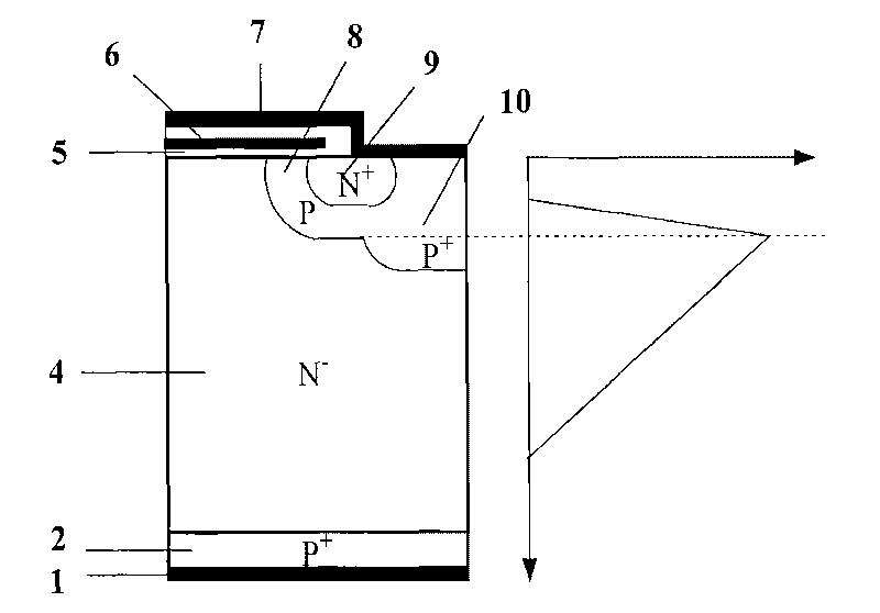
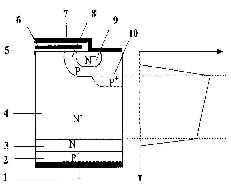
[0035] A slot gate IGBT with a P-type floating layer, such as Figure 6 As shown, each cell includes collector 1, P + Collector area 2, N - Base region 4, gate oxide layer 5, polysilicon gate 6, emitter 7, N + Source region 9, P + Body region 10 and P-type floating layer 11.

[0036] The gate oxide layer 5 and the polysilicon gate 6 form a trench structure, and the trench structure is located in the cell N - The middle and upper part of the base region 4, and the oxid...


PUM


Abstract

The invention relates to a grooved gate IGBT with a P-type floating layer, belonging to the technical filed of semiconductor power devices. On a basis of grooved gate insulated-gate bipolar transistor (IGBT) controlled by an accumulation layer, a P-type floating layer (11) is introduced to effectively improve the electric-field integration effect of the bottom of the grooved gate and greatly increase the breakdown voltage of the device. Meanwhile, due to the existence of the P-type floating layer, a JFET zone is introduced to play the effect of shielding the groove barrier potential of the accumulation layer to a certain extent and greatly reduce the drain current of the device. When the device is forwardly conducted, the saturation current density of the device is greatly decreased so as to greatly improve the short-circuit safety operation area (SCSOA) of the device. The invention maintains the original low forward-conducted voltage drop of the grooved gate IGBT controlled by the accumulation layer and increases the forward bias safety operation area (FBSOA) and the bolt current density while decreasing the drain current of the device, improving the breakdown voltage of the device and greatly improving the SCSOA of the device.

Description

technical field [0001] A slot gate IGBT with a P-type floating layer belongs to the technical field of semiconductor power devices. Background technique [0002] Insulated gate bipolar transistor is a rapidly developing and widely used power electronic device. It is a new device combined with the advantages of high input impedance of MOSFET, simple driving circuit, high current density and low saturation voltage of bipolar transistor. Now it is widely used in induction cooker, UPS uninterruptible power supply, automotive electronic igniter, frequency converter, motor transmission system and other energy conversion devices. [0003] IGBT was first proposed in 1982 as a punch-through structure, such as figure 1 As shown, it is at high concentrations of P + Substrate (P + Collector region) 2 epitaxial N-type buffer layer 3, N - The base region layer 4 is fabricated into an insulated gate bipolar transistor structure. Due to the presence of the N-type buffer layer 3, the e...

Claims


Application Information

Patent Timeline
Patent Type & Authority Applications(China)
IPC IPC(8): H01L29/739H01L29/06H01L27/04
Inventor 李泽宏钱梦亮王蓉张波
Owner UNIV OF ELECTRONICS SCI & TECH OF CHINA
Why Eureka
Try Eureka