Micro hole manufacturing process of multilayer HDI circuit board

A manufacturing process and circuit board technology, applied in the direction of electrical connection formation of printed components, etc., can solve problems such as unstable performance, difficult processing of circuit board microholes, etc., and achieve the effect of improving wiring density

Inactive Publication Date: 2010-05-19
惠州中京电子科技股份有限公司
View PDF0 Cites 20 Cited by
  • Summary
  • Abstract
  • Description
  • Claims
  • Application Information

AI Technical Summary

Problems solved by technology

[0003] The present invention aims to solve the problems of difficult processing and unstable performance of circuit board micro-holes in the prior art, and further provide a circui

Method used


Image

  • Micro hole manufacturing process of multilayer HDI circuit board
  • Micro hole manufacturing process of multilayer HDI circuit board

Examples


Embodiment Construction

[0016] In order to facilitate the understanding of those skilled in the art, the present invention will be described in further detail below in conjunction with specific embodiments:

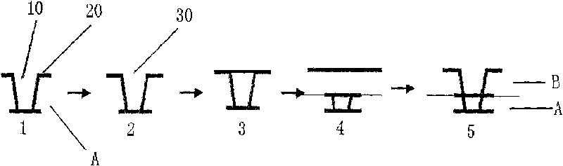
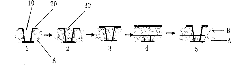
[0017] The micropore manufacturing process of the multilayer HDI circuit board is:

[0018] (1) Laser drilling the inner circuit board and electroplating the hole wall;

[0019] (2) Carry out resin plugging to the microhole or microthrough hole after electroplating;

[0020] (3) Orifice resin grinding;

[0021] (4) Copper sinking and electroplating are carried out on the polished orifice resin surface to metallize the orifice resin surface;

[0022] (5) Inner layer circuit etching and outer layer lamination;

[0023] (6) Laser drilling and electroplating on the outer layer;

[0024] (7) Perform graphic electroplating on the outer layer board to realize electrical interconnection between layers.

[0025] Three key technologies need to be overcome in the micro-hole manufacturing process of th...


PUM

PropertyMeasurementUnit
Hardnessaaaaaaaaaa

Abstract

The invention discloses a micro hole manufacturing process of a multilayer HDI circuit board. The process comprises the following steps of: (1) carrying out inner-layer laser hole drilling and electroplating; (2) stuffing the electroplated micro holes or micro through holes by resin; (3) grinding orifice resin; (4) carrying out copper deposition and electroplating on the ground orifice resin after stuffing the holes so as to ensure that the surface of the orifice resin is metallized; (5) carrying out inner-layer circuit board etching and outer-layer lamination; (6) carrying out outer-layer laser hole drilling; and (7) electroplating outer-layer patterns to realize interlaminar electrical interconnection. The process breaks a conventional processing mode of micro hole filling and electroplating at present and adopts the method of electroplating after laser hole drilling, stuffing the holes and then electroplating to realize the interlaminar electrical interconnection of PCB boards. The process can realize micro hole overlapping and interconnection and the resetting of welding points on the surfaces of the through holes, can further improve the wiring density of inner-layer and outer-layer circuit boards and is beneficial to developing the PCB boards to miniaturization, densification and high reliability.

Description

technical field [0001] The invention relates to the technical field of printed circuit boards, in particular to a microhole manufacturing process of a multi-layered HDI printed circuit board. Background technique [0002] With the rapid development of electronic technology, electronic products tend to be miniaturized, portable, and highly integrated, and the packaging of semiconductor components also tends to be multi-pin and fine-pitched. Smaller, lighter and denser. Whether the PCB substrate can be high-density depends on the micro-holes and lines connected between layers, and it depends on the performance of electronic products. Therefore, micro-hole technology in the PCB industry has become one of the key technologies in the PCB industry. Microvias include through holes, buried holes and blind holes on printed circuit boards. In the industry, the commonly used micro-hole manufacturing process is to use conductive rubber particles to plug holes to realize interlayer ele...

Claims


Application Information

Patent Timeline
IPC IPC(8): H05K3/42
Inventor 周刚
Owner 惠州中京电子科技股份有限公司
Why Eureka
Try Eureka