

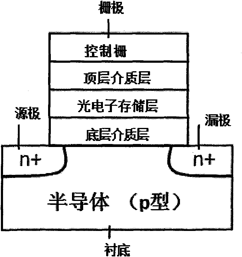
Signal read-out amplifying method of photosensitive compound medium grid MOSFET detector
A composite medium and readout amplification technology, which is applied in image communication, semiconductor devices, electrical components, etc., can solve the problems of low yield, difficulty in improving imaging speed, and high production cost.
- Summary
- Abstract
- Description
- Claims
- Application Information
AI Technical Summary
Problems solved by technology
Method used
Image

Examples
Embodiment Construction
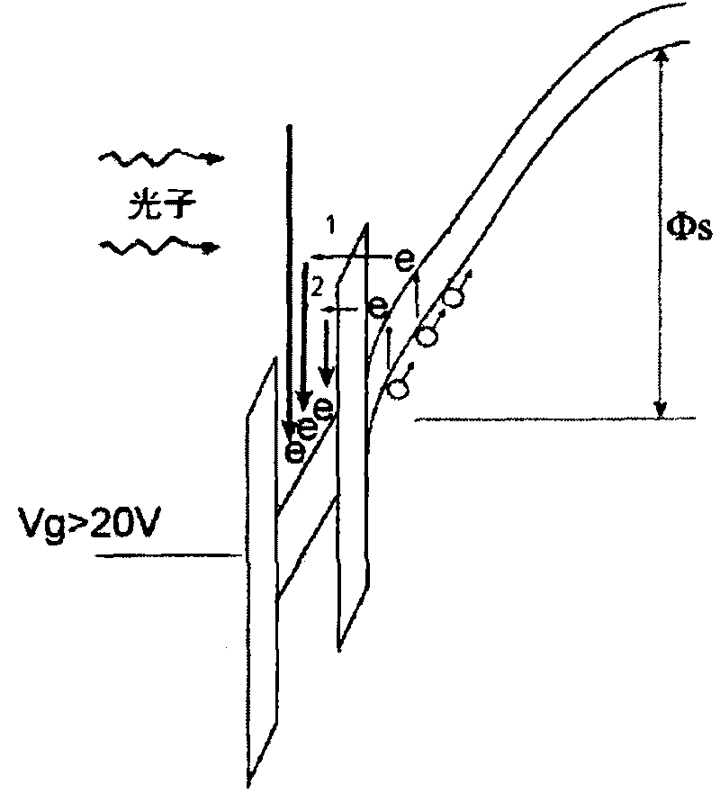
[0050] 1. The detector works in the linear region
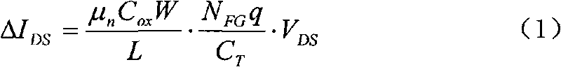
[0051] Connect the source and substrate of the detector to ground, and connect the drain to a suitable positive voltage V D , by adjusting the gate voltage V G Make the detector work in the linear region. By directly measuring the output drain current, that is, comparing the two values of the drain current before and after exposure to determine the size of the optical signal, the relationship between the amount of drain current change and the number of photoelectrons collected is as follows:
[0052] ΔI DS = μ n C ox W L · N FG q C T · V DS - - - ( ...
PUM
 Abstract
Description
Claims
Application Information