Method for removing photoresist and plasma processing equipment applying same

A technology of photoresist and process gas, which is applied in the field of microelectronics, can solve the problems of difficulty and damage in effectively and uniformly removing photoresist, so as to avoid damage to the surface of silicon wafers, remove evenly, and improve production efficiency and processing quality effects

Inactive Publication Date: 2010-06-16
BEIJING NAURA MICROELECTRONICS EQUIP CO LTD
View PDF0 Cites 1 Cited by
  • Summary
  • Abstract
  • Description
  • Claims
  • Application Information

AI Technical Summary

Problems solved by technology

[0005] In practical applications, the photoresist on the surface needs to be removed to obtain the finished silicon wafer. However, after plasma etching or ion implantation, a carbon-rich structure with a certain thickness will be formed on the surface of the photoresist. Or a hardened layer similar to a carbon-rich structure, which makes it difficult to remove the photoresist effectively and uniformly, and also damages the silicon wafer (the silicon wafer mentioned herein includes the dielectric) during the removal of the photoresist layer and polysilicon / monocrystalline silicon layer) surface damage

Method used


Image

  • Method for removing photoresist and plasma processing equipment applying same
  • Method for removing photoresist and plasma processing equipment applying same
  • Method for removing photoresist and plasma processing equipment applying same

Examples


Embodiment Construction

[0030] In order to enable those skilled in the art to better understand the technical solutions of the present invention, the method for removing photoresist provided by the present invention and the plasma processing equipment applying the method will be described in detail below with reference to the accompanying drawings.

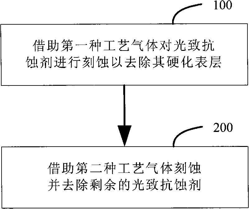
[0031] See figure 2 The method for removing photoresist provided by the present invention mainly includes the following steps:

[0032] 100) In the reaction chamber, the photoresist on the surface of the silicon wafer is etched with the aid of the first process gas, so as to remove at least the hardened layer on the photoresist.

[0033] 200) Continue to etch the photoresist with the aid of the second process gas to remove the remaining photoresist.

[0034] Wherein, the composition of the first process gas used in step 100) includes O 2 , CHxFy, N 2 , CO 2 Wait for the gas, here, O 2 And CHxFy is the main component, indispensable; and N 2 And CO 2 It can be add...


PUM


Abstract

The invention provides a method for removing a photoresist, comprising the following steps of: (100) etching the photoresist positioned on the surface of a silicon wafer by means of a first process gas so as to at least remove a hardened layer of the photoresist; and (200) continuously etching the photoresist by means of a second process gas so as to remove the rest photoresist. Besides, the invention also provides plasma processing equipment applying the method for removing the photoresist. The method for removing the photoresist and the plasma processing equipment can fast and uniformly remove the photoresist positioned on the surface of the silicon wafer, effectively reduce and even prevent the damage to the surface of the silicon wafer and also enhances the production efficiency, the processing quality, and the like.

Description

Technical field [0001] The present invention relates to the field of microelectronics technology, and in particular, to a method for removing photoresist and a plasma processing device applying the method. Background technique [0002] With the advancement of science and technology, large-scale integrated circuits have been applied to various fields of social production, and their requirements for integration and processing accuracy are getting higher and higher. Semiconductor processing companies must continuously improve their own production capacity and processing quality to meet new market demands. [0003] The processing of semiconductor devices is a process in which photoresist is used as an intermediate medium and its anti-corrosion performance is used to achieve pattern transformation, transfer and processing, and finally to transfer the pattern information to the silicon wafer. The processing process includes: ①Pattern transfer process, uniformly coating photoresist on th...

Claims


Application Information

Patent Timeline
IPC IPC(8): G03F7/36G03F7/42H05H1/00
Inventor 朱哲渊
Owner BEIJING NAURA MICROELECTRONICS EQUIP CO LTD
Why Eureka
Try Eureka