Method for fabricating bump

A fabrication method and bump technology, applied in semiconductor/solid-state device manufacturing, electrical components, electrical solid-state devices, etc., can solve problems such as affecting reliability, short-circuiting semiconductor devices, affecting the electrical properties of copper metal layers, etc., to achieve reliability assurance , avoid short circuit, the effect of improving electrical performance

Inactive Publication Date: 2010-06-16
SEMICON MFG INT (SHANGHAI) CORP +1
View PDF0 Cites 9 Cited by
  • Summary
  • Abstract
  • Description
  • Claims
  • Application Information

AI Technical Summary

Problems solved by technology

[0007] In the process of reflow forming bumps in the prior art, since the chip is placed on the hot plate, after the reflow process, due to gravity and surface tension, the bump material will penetrate into the UBM layer in (such as Figure 4 shown in the middle circle), thereby reducing the quality of the metal layer under the bump and affecting its reliability; in addition, during the production process of the copper pillar bump, there is a thicker layer of copper metal layer under the bump, and the chip When placed on a hot plate, when the reflowed solder layer forms a bump, due to the effect of gravity, the bump material will flow to the edge of the copper metal layer (such as Figure 5 shown in the middle ellipse), which affects the electrical properties of the copper metal layer; also due to the effect of gravity and surface tension, the bumps formed after reflow are generally elliptical rather than circular, because the integration of semiconductor devices is getting higher and higher. The spacing between the bumps is getting smaller and smaller, therefore, it is easy to generate bridges between the bumps, causing short circuits between semiconductor devices

Method used


Image

  • Method for fabricating bump
  • Method for fabricating bump
  • Method for fabricating bump

Examples


Embodiment Construction

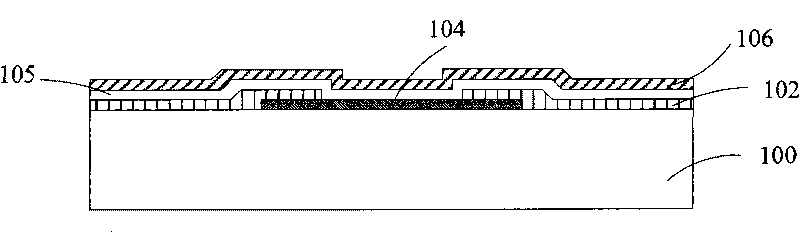
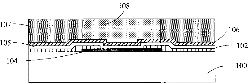
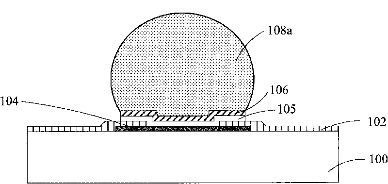
[0022] Flip-chip technology is gaining more and more attention because it can reduce the size of the package. As a key technology in flip-chip manufacturing technology, the quality of bump production directly affects the quality of flip-chip. In the invention, the opposite surface of the surface where the solder layer of the chip is located is in contact with and fixed to the hot plate of the reflow furnace, and the chip is located under the hot plate. Due to the inversion of the solder layer, the solder layer will only flow downward under the influence of gravity during the reflow process, and will not penetrate into the UBM layer, so that the reliability of the UBM layer is guaranteed; at the same time, the solder layer After inversion, the bumps formed by reflow will not produce bridging phenomenon, avoiding the occurrence of short circuit; in the process of making copper pillar bumps, the inversion of the solder layer will prevent the solder layer from flowing along the ed...


PUM

PropertyMeasurementUnit
thicknessaaaaaaaaaa
thicknessaaaaaaaaaa
thicknessaaaaaaaaaa

Abstract

The invention discloses a method for fabricating a bump. The method comprises the following steps of: providing a chip on which a solder layer is formed; placing the chip in a refluxing device, wherein the solder layer is positioned below the surface of the chip; and refluxing the solder layer to form the bump. The method for fabricating the bump ensures the reliability of a metal layer below the bump; the bump does not cause a bridging phenomenon so as to avoid a short circuit; and the electrical property of a copper metal layer is improved in the fabricating process of the bump of a copper cylinder.

Description

technical field [0001] The invention relates to the field of manufacturing semiconductor devices, in particular to a method for manufacturing bumps. Background technique [0002] With the continuous development of integrated circuit technology, electronic products are increasingly developing in the direction of miniaturization, intelligence, high performance and high reliability. The integrated circuit packaging not only directly affects the performance of integrated circuits, electronic modules and even the whole machine, but also restricts the miniaturization, low cost and reliability of the entire electronic system. With the gradual reduction of the size of the integrated circuit chip and the continuous improvement of the integration level, the electronic industry has put forward higher and higher requirements for the integrated circuit packaging technology. [0003] Flip chip (flip chip) technology is through the solder balls formed on the surface of the chip, so that t...

Claims


Application Information

Patent Timeline
Patent Type & Authority Applications(China)
IPC IPC(8): H01L21/60
CPCH01L24/11H01L2224/11H01L2924/14H01L2924/00H01L2924/00012
Inventor 丁万春孟津
Owner SEMICON MFG INT (SHANGHAI) CORP
Why Eureka
Try Eureka