Substrate modification-based method for preparing anisotropic organic field effect transistor

An anisotropic and organic field technology, applied in semiconductor/solid-state device manufacturing, semiconductor devices, electrical components, etc., can solve the problems of uneven film performance, easy introduction of impurities, poor repeatability, etc., to achieve high uniformity and artificial High controllability and good repeatability

Inactive Publication Date: 2010-06-16
INST OF MICROELECTRONICS CHINESE ACAD OF SCI
View PDF0 Cites 0 Cited by
  • Summary
  • Abstract
  • Description
  • Claims
  • Application Information

AI Technical Summary

Problems solved by technology

This method has low controllability, poor repeatability, uneven film properties and easy introduction of impurities

Method used


Image

  • Substrate modification-based method for preparing anisotropic organic field effect transistor
  • Substrate modification-based method for preparing anisotropic organic field effect transistor
  • Substrate modification-based method for preparing anisotropic organic field effect transistor

Examples


Embodiment Construction

[0026] In order to make the object, technical solution and advantages of the present invention clearer, the present invention will be described in further detail below in conjunction with specific embodiments and with reference to the accompanying drawings.

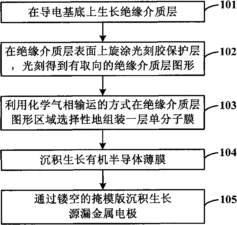
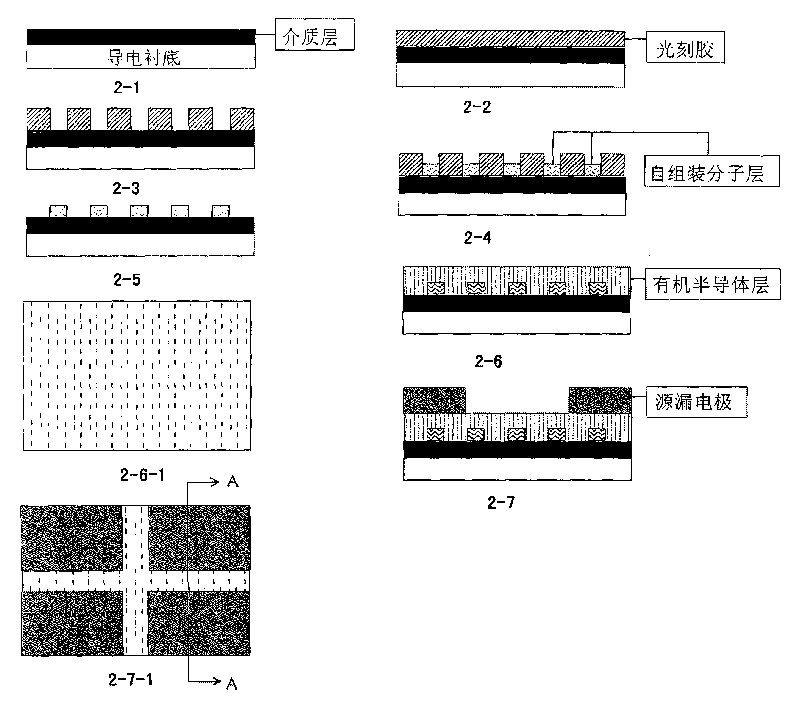
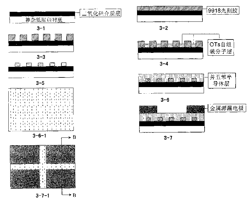
[0027] like figure 1 as shown, figure 1 It is a flowchart of the method for preparing an anisotropic organic field effect transistor based on substrate modification provided by the present invention. The method is to modify the substrate by one-time insulating medium layer growth, one-time photolithography, one-time monolayer molecular self-assembly, and one-time organic semiconductor thin film Growth and primary metal deposition to obtain an anisotropic organic field effect tube, specifically including the following steps:

[0028] Step 101: growing an insulating dielectric layer on a conductive substrate;

[0029] Step 102: Spin-coat a photoresist protective layer on the surface of the insulating dielectric layer, and...


PUM


Abstract

The invention discloses a substrate modification-based method for preparing an anisotropic organic field effect transistor. The anisotropic organic field effect transistor is obtained through the primary growth of an insulating medium layer, primary photoetching, primary self-assembling substrate modification by single-layer molecules, primary growth of an organic semiconductor film and primary metal deposition. The method particularly comprises the following steps of: growing the insulating medium layer on an electrically-conductive substrate; spin coating a photoresist protective layer on the surface of the insulating medium layer to obtain an oriented insulating medium layer pattern; selectively assembling a layer of monomolecular film in a region of the insulating medium layer pattern in a chemical vapor transportation mode; growing the organic semiconductor film through deposition; and growing source and drain metal electrodes through deposition by a hollow mask. The substrate modification-based method for preparing the anisotropic organic field effect transistor has the advantages of simple process, high artificial controllability, good repeatability and high uniformity, wherein the anisotropic organic field effect transistor is high in mobility.

Description

technical field [0001] The invention relates to the technical field of microfabrication in organic semiconductors, in particular to a method for preparing anisotropic organic field effect transistors based on substrate modification. Background technique [0002] With the deepening of information technology, electronic products have entered every aspect of people's life and work. In daily life, people's demand for low-cost, flexible, low-weight, and portable electronic products is increasing. Traditional devices and circuits based on inorganic semiconductor materials are difficult to meet these requirements. Therefore, organic microelectronics technology based on semiconductor materials such as organic polymers and organic small molecules that can achieve these characteristics has gained more and more people under this trend. s concern. Improving the mobility of organic field effect transistors and studying the intrinsic properties of organic semiconductors have always been...

Claims


Application Information

Patent Timeline
Patent Type & Authority Applications(China)
IPC IPC(8): H01L51/40
Inventor 姬濯宇商立伟刘明
Owner INST OF MICROELECTRONICS CHINESE ACAD OF SCI
Why Eureka
Try Eureka