SCR ESD protective structure with high maintaining voltage

A high maintenance voltage, electrostatic discharge protection technology, applied in emergency protection circuit devices, emergency protection circuit devices, circuits, etc. for limiting overcurrent/overvoltage, which can solve the problem of increasing device size and reducing secondary thermal shock Through the failure current, increase the maintenance voltage and other problems, to achieve the effect of eliminating the latch-up effect and good ESD protection ability

Inactive Publication Date: 2010-06-30
SUZHOU POWERON IC DESIGN
View PDF0 Cites 17 Cited by
  • Summary
  • Abstract
  • Description
  • Claims
  • Application Information

AI Technical Summary

Problems solved by technology

[0006] In related technologies, it has been proposed to increase the holding voltage by increasing the distance between the anode and the cathode to prevent latch-up, but this will increase the size of the de...

Method used


Image

  • SCR ESD protective structure with high maintaining voltage
  • SCR ESD protective structure with high maintaining voltage
  • SCR ESD protective structure with high maintaining voltage

Examples


Embodiment Construction

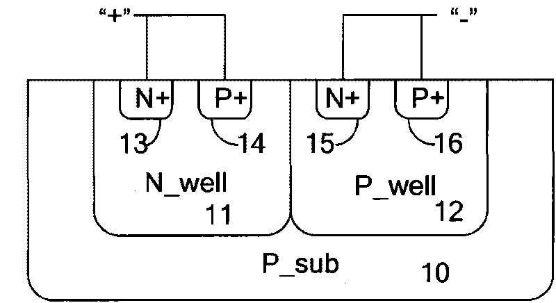
[0022] figure 1 It is a schematic cross-sectional view of a traditional lateral SCR. This is a double-well device manufactured on a P-type substrate 10. On the substrate 10 are an N-type well 11 and a P-type well 12. The N-type well 11 is connected to the P+ doped region 14 through an N+ doped region 13. , as the anode of the SCR, the P-type well 12 is connected to the P+ doped region 16 through the N+ doped region 15, and serves as the cathode of the SCR; the P+ doped region 14, the N-type well 11, the P-type well 12, and the N+ doped region Region 15 constitutes the structure of the PNPN.

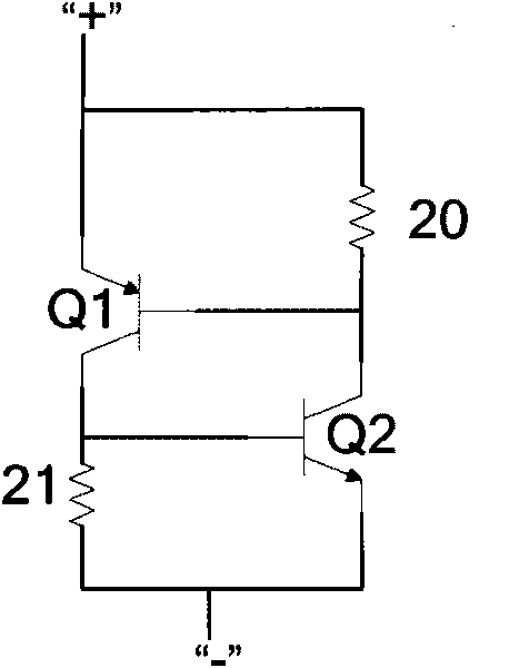
[0023] figure 2 yes figure 1 The equivalent circuit diagram of the structure shown includes a parasitic PNP transistor Q1 and a parasitic NPN transistor Q2, N well resistor 20 and P well resistor 21.

[0024] In a traditional CMOS process, both the PNP transistor Q1 and the NPN transistor Q2 are parasitic devices, and the emitter, collector, and base of the parasitic PNP transistor Q...


PUM


Abstract

The invention relates to an electrostatic discharge protective SCR structure with high maintaining voltage, which is formed on a device; the device comprises a P-type substrate, an N type buried layer is arranged on the P-type substrate, an N type well is arranged on the N type buried layer, a P-type well parallel to the N type well is also arranged on the P-type substrate, a first N+ doping region and a first P+ doping region are arranged in the N type well, the first N+ doping region and the first P+ doping region are led out through a contact hole and are connected together for being used as the anode of the device, a second N+ doping region and a second P+ doping region are arranged in the P+ doping region, the second N+ doping region and the second P+ doping region are led out through the contact hole and are connected together for being used as the cathode of the device. The SCR structure is composed of the P+ doping region, the N+ doping region and the P-type well region in the N type well and the N+ doping region in the P-type well, the N well resistance is increased by the buried layer between the P-type substrate and the N type well under a maintaining state, so as to increase the maintaining voltage.

Description

technical field [0001] The present invention relates to electrostatic discharge (ESD) protection using semiconductor controlled rectifier (SCR) devices, and more specifically relates to a SCR ESD protection structure with high sustain voltage. Background technique [0002] With the continuous development of integrated structure technology, the feature size of integrated structure is gradually reduced. Advanced technologies such as short gate length, thin gate oxide layer, shallow junction depth, lightly doped drain region and silicide doping are improving the performance of integrated structure and At the same time, the integration level causes the internal structure to be more easily damaged when the electrostatic discharge ESD strikes. According to statistics, the economic losses caused by ESD in the semiconductor industry are calculated in billions of dollars every year. Therefore, disposing an ESD protection structure at each input and output port becomes one of the eff...

Claims


Application Information

Patent Timeline
IPC IPC(8): H01L29/74H01L29/06H01L23/60H02H9/00
CPCH01L29/87H01L29/1016
Inventor 易扬波杨东林祝靖王钦刘侠
Owner SUZHOU POWERON IC DESIGN
Why Eureka
Try Eureka