A kind of hk SOI LDMOS device with tri-gate structure

A gate structure and device technology, applied in semiconductor devices, electrical components, circuits, etc., can solve the problems of high power consumption, large specific on-resistance, etc., to eliminate latch-up effects, increase channel density, and improve doping Effect

Active Publication Date: 2018-10-26
UNIV OF ELECTRONICS SCI & TECH OF CHINA
View PDF2 Cites 0 Cited by
  • Summary
  • Abstract
  • Description
  • Claims
  • Application Information

AI Technical Summary

Problems solved by technology

The literature (Variation of lateral width technique in SoI high-voltage lateral double-diffused metal–oxide–semiconductor transistors using high-kdielectric, IEEE Electron Device Letter, vol.36, no.3, 2015) introduces a variable width high in the drift region K medium greatly improves the withstand voltage of the device, but the specific on-resistance of the device is still large and the power consumption is high.

Method used


Image

  • A kind of hk SOI LDMOS device with tri-gate structure
  • A kind of hk SOI LDMOS device with tri-gate structure
  • A kind of hk SOI LDMOS device with tri-gate structure

Examples


Embodiment 1

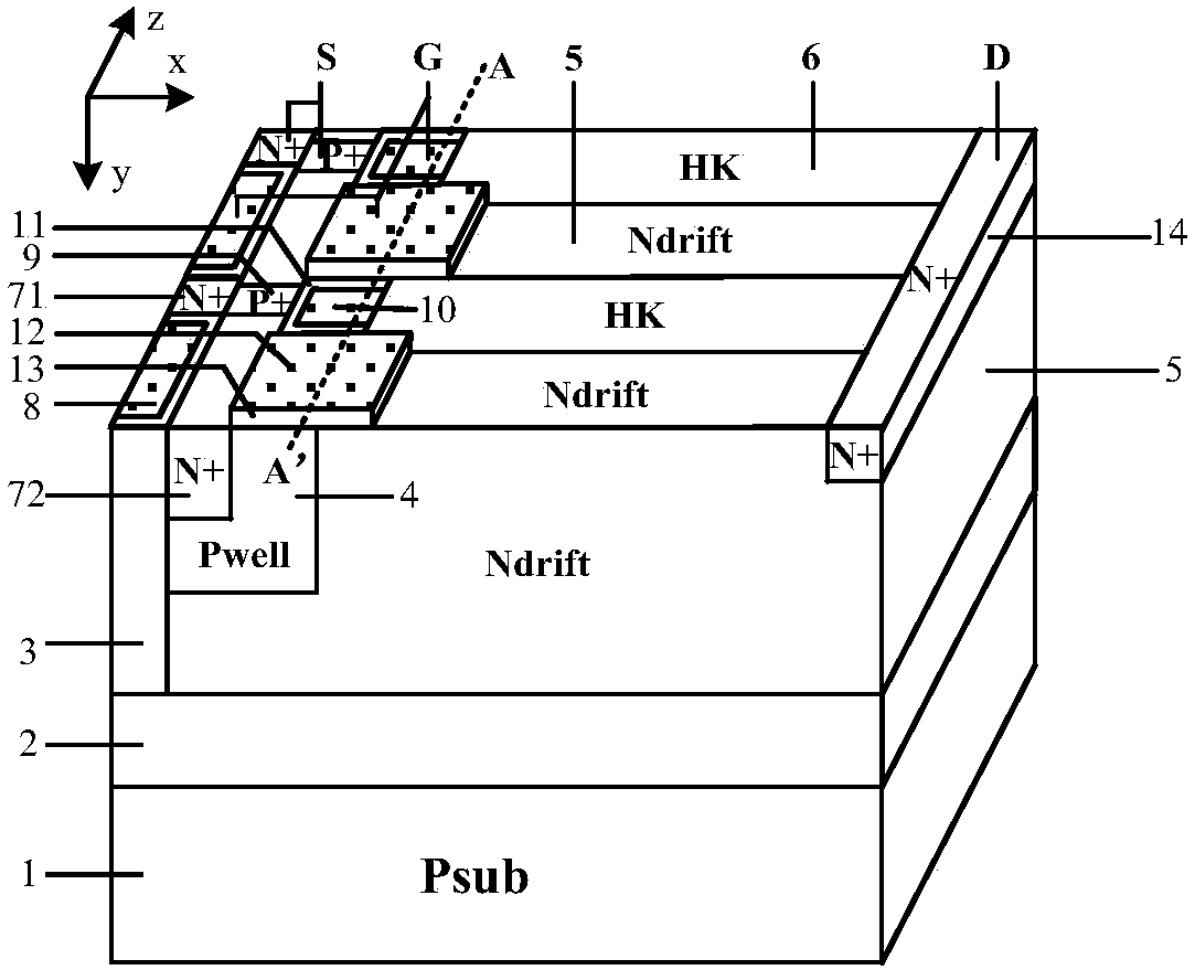
[0027] Such as figure 1As shown, the specific structure of this example includes a second conductivity type semiconductor substrate layer 1 and a dielectric buried layer 2 above it; the upper surface of the dielectric buried layer 2 has a first conductivity type semiconductor drift region 5, and the upper layer of the drift region 5 is One side has a semiconductor body region 4 of the second conductivity type, and a high-K dielectric 6 is embedded in the drift region 5 close to the semiconductor body region 4. The high-K dielectric 6 and the drift region 5 are arranged alternately in the longitudinal direction, and the high-K dielectric It is a material with a dielectric constant greater than 3.9; a first trench gate structure extending to the dielectric buried layer 2 is formed through the side of the semiconductor body region 4 away from the drift region 5, and the first trench gate structure includes a first The trench gate dielectric 3 and the first conductive material 8 s...

Embodiment 2

[0030] Such as image 3 As shown, compared with Embodiment 1 in this example, the first trench gate structure is vertically segmented, and the upper layer of the semiconductor body region 4 between every two first trench gate structures has the second conductivity type The heavily doped semiconductor body contact region 9; on the side of the upper layer of the semiconductor body region 4 that is in contact with the first trench gate, there is a heavily doped semiconductor source region 72 of the first conductivity type, and the source structure includes heavy doped semiconductors of the first conductivity type. The doped semiconductor source region 72 and the second conductivity type heavily doped semiconductor body contact region 9 .

[0031] Compared with Embodiment 1, in this example, the heavily doped semiconductor source region of the first conductivity type and the body contact region of the heavily doped semiconductor of the second conductivity type can be formed by ion...

Embodiment 3

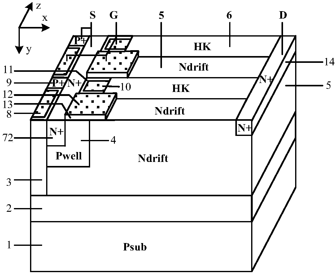
[0033] Such as Figure 4 As shown, compared with Embodiment 1 in this example, the first trench gate structure is continuous in the vertical direction; the upper layer of the semiconductor body region 4 between the first trench gate and the planar gate is of the first conductivity type The heavily doped semiconductor source region 72, the upper layer of the semiconductor body region 4 between the first trench gate and the second trench gate is the second conductivity type heavily doped semiconductor body contact region 9, the source structure includes the first A heavily doped semiconductor source region 72 of a conductivity type and a body contact region 9 of a second conductivity type heavily doped semiconductor.

[0034] Compared with Embodiment 1, in this example, the first trench gate structure is continuous, and it can be used as a dielectric isolation layer in the low-voltage area of ​​the integrated circuit, which facilitates the isolation of high-voltage and low-volta...


PUM


Abstract

The invention belongs to the technical field of semiconductors, and in particular relates to an HK SOI LDMOS device with a triple gate structure. The present invention has the following characteristics: 1. It has three separate gate structures, including a planar gate and two trench gates. In the open state, the triple gate structure can form multiple channels including horizontal and vertical , increase the channel density, increase the current, and reduce the specific on-resistance; 2. Embed high-K dielectrics from the drift region close to the semiconductor body region, which are arranged alternately with the drift region in the vertical direction, and close to the high-K in the on-state The electron accumulation layer is formed on the side wall of the drift region, which provides a low-resistance channel and reduces the specific on-resistance. In the off state, the high-K dielectric assists in depleting the drift region, increasing the doping of the drift region, and improving the electric field, further reducing the specific on-resistance and improving Withstand voltage; 3. Adopt SOI structure, improve vertical withstand voltage, reduce leakage current, and eliminate latch-up effect.

Description

technical field [0001] The invention belongs to the technical field of semiconductors, and in particular relates to an HK SOI LDMOS device with a triple gate structure. Background technique [0002] LDMOS (Lateral Double-diffusion Metal Oxide Semiconductor, lateral double-diffusion metal-oxide-semiconductor field) is a multi-subconduction device with high input impedance, fast switching speed, and easy integration. It is used in intelligent power integrated circuits widely used. For LDMOS, high withstand voltage (BV) means longer drift region length and lower drift region doping, which also leads to specific on-resistance (R on,sp ) is greatly increased, therefore, the silicon limit problem (R on,sp ∝BV 2.5 ) seriously restricts the development of LDMOS devices. [0003] For low withstand voltage (BV<200V) devices, the channel resistance becomes an important factor of conduction power consumption, so how to reduce the channel resistance of the device has become a rese...

Claims


Application Information

Patent Timeline
Patent Type & Authority Patents(China)
IPC IPC(8): H01L29/06H01L29/10H01L29/423H01L29/78
CPCH01L29/0684H01L29/1037H01L29/4236H01L29/7824H01L29/7825H01L29/7831
Inventor 罗小蓉吕孟山尹超魏杰谭桥周坤葛薇薇何清源
Owner UNIV OF ELECTRONICS SCI & TECH OF CHINA
Why Eureka
Try Eureka