Molding structure and method for laser-assisting base plate line

A laser-assisted, substrate technology, used in the improvement of metal adhesion of insulating substrates, circuits, and secondary processing of printed circuits, etc., can solve the problems of short circuit, open circuit, circuit peeling, etc. The effect of reducing process costs

Active Publication Date: 2010-06-30
NAN YA PRINTED CIRCUIT BOARD CORPORATION
View PDF0 Cites 6 Cited by
  • Summary
  • Abstract
  • Description
  • Claims
  • Application Information

AI Technical Summary

Problems solved by technology

[0004] In addition, when the structure evolves to a fine line, it is easy to cause the line to peel off due to poor bonding force between the line and the insulating layer, which will cause a short circuit or open circuit, and the circuit board will be scrapped

Method used


Image

  • Molding structure and method for laser-assisting base plate line
  • Molding structure and method for laser-assisting base plate line
  • Molding structure and method for laser-assisting base plate line

Examples


Embodiment Construction

[0026] The laser-assisted circuit forming method of the substrate according to the embodiment of the present invention will be described in detail below with reference to the accompanying drawings. It should be noted that the above-mentioned drawings are all simplified schematic diagrams to emphasize the features of the present invention, so the dimensions of the components in the drawings are not completely drawn according to actual scale. And the embodiments of the present invention may also include elements not shown in the figures.

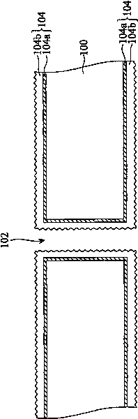
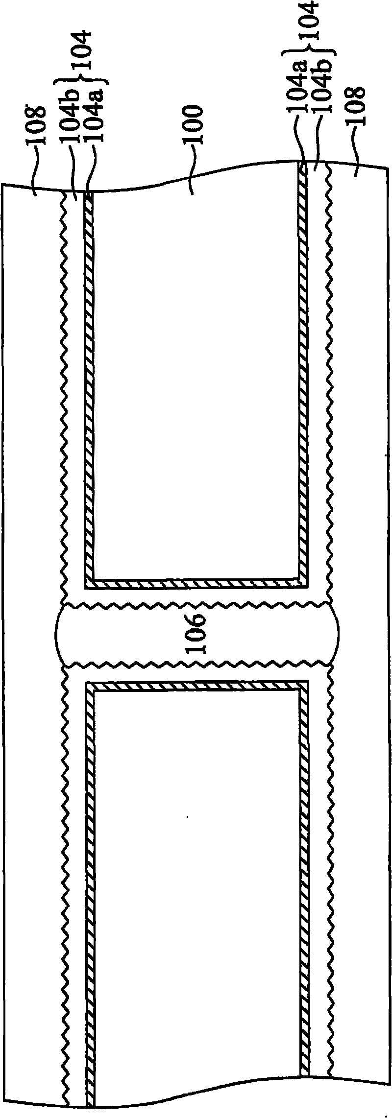
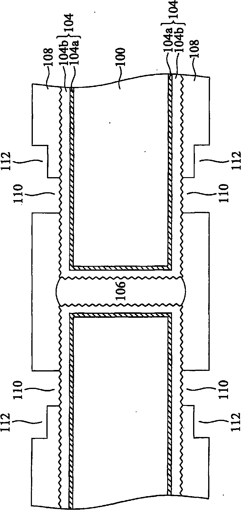
[0027] see Figure 1 to Figure 5 , an embodiment of the method for providing laser-assisted circuit formation on a substrate in the present invention will be described in detail. See figure 1 , first provide a circuit substrate 100 containing a plurality of through holes (through hole) 102, wherein the circuit substrate 100 includes paper phenolic resin (paper phenolic resin), composite epoxy resin (composite epoxy), polyimide resin (polyim...


PUM

PropertyMeasurementUnit
thicknessaaaaaaaaaa

Abstract

The invention provides a molding structure and a method for a laser-assisting base plate line; wherein the method comprises the following steps: providing a circuit base plate provided with multiple via holes; forming a first metal layer on the multiple via holes and the circuit base plate; forming a dielectric layer coating the first metal layer; carrying out laser hole drilling to form multiple via holes and grooves in the dielectric layer, wherein the multiple via holes expose the first metal layer, the multiple grooves are arranged above the via holes; forming a second metal layer between the multiple via holes and the multiple grooves to electrically connect the second metal layer to the first metal layer. The invention has the following advantages of saving publicly known image transferring process, simplifying processing steps and lowering processing cost, increasing binding force between the metal layers and the dielectric layer and solving the problem that the line is peeled off due to bad binding force between the line and an insulation layer.

Description

technical field [0001] The invention relates to a circuit forming structure and method, in particular to a laser-assisted substrate circuit forming structure and method. Background technique [0002] In the new generation of electronic products, the continuous pursuit of lightness, thinness and smallness has led to the development of integrated circuits (Integrated Circuit, IC) towards high density. The configuration of sexual connection lines is more intensive. [0003] At present, image transfer technology is often used to make connection lines. The so-called image transfer technology is a series of processes of applying photoresist, exposure, development, electroplating, film removal and etching to pattern the required lines. However, using In image transfer technology, each step in the process needs to be optimally controlled, especially for fine lines, the process needs to be controlled more precisely to obtain the desired lines. [0004] In addition, when the structu...

Claims


Application Information

Patent Timeline
Patent Type & Authority Applications(China)
IPC IPC(8): H05K3/42H05K3/38H01L21/48H01L23/498
Inventor 吴明松林世宗林贤杰江国春何信芳
Owner NAN YA PRINTED CIRCUIT BOARD CORPORATION
Why Eureka
Try Eureka