Grooved semiconductor rectifier and manufacturing method thereof

A manufacturing method and semiconductor technology, applied in semiconductor/solid-state device manufacturing, semiconductor devices, electric solid-state devices, etc., can solve the problem of inability to achieve high reverse blocking voltage, reduce forward conduction voltage drop, unfavorable trench etching, etc. problem, to achieve the effect of simple manufacturing process, reduced forward voltage drop, and low cost

Inactive Publication Date: 2010-07-21
无锡新洁能功率半导体有限公司
View PDF4 Cites 24 Cited by
  • Summary
  • Abstract
  • Description
  • Claims
  • Application Information

AI Technical Summary

Problems solved by technology

[0006] However, since many rectifier applications need to be able to withstand a high blocking voltage in the reverse direction and have a low conduction voltage drop during forward conduction, if the drift region of the first conductivity type in the above patent structure is selected as Higher resistivity and thicker thickness are not conducive to reducing the forward voltage drop, and are not conducive to the realization of trench etching extending into the substrate layer; If it is thinner, it cannot achieve high reverse blocking voltage

Method used


Image

  • Grooved semiconductor rectifier and manufacturing method thereof
  • Grooved semiconductor rectifier and manufacturing method thereof
  • Grooved semiconductor rectifier and manufacturing method thereof

Examples


Embodiment Construction

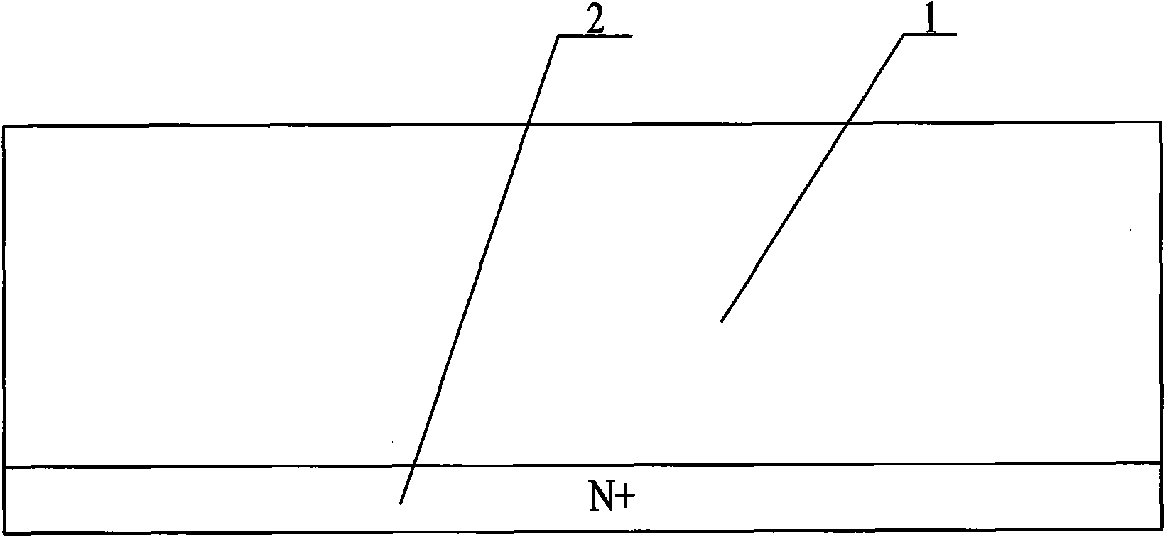
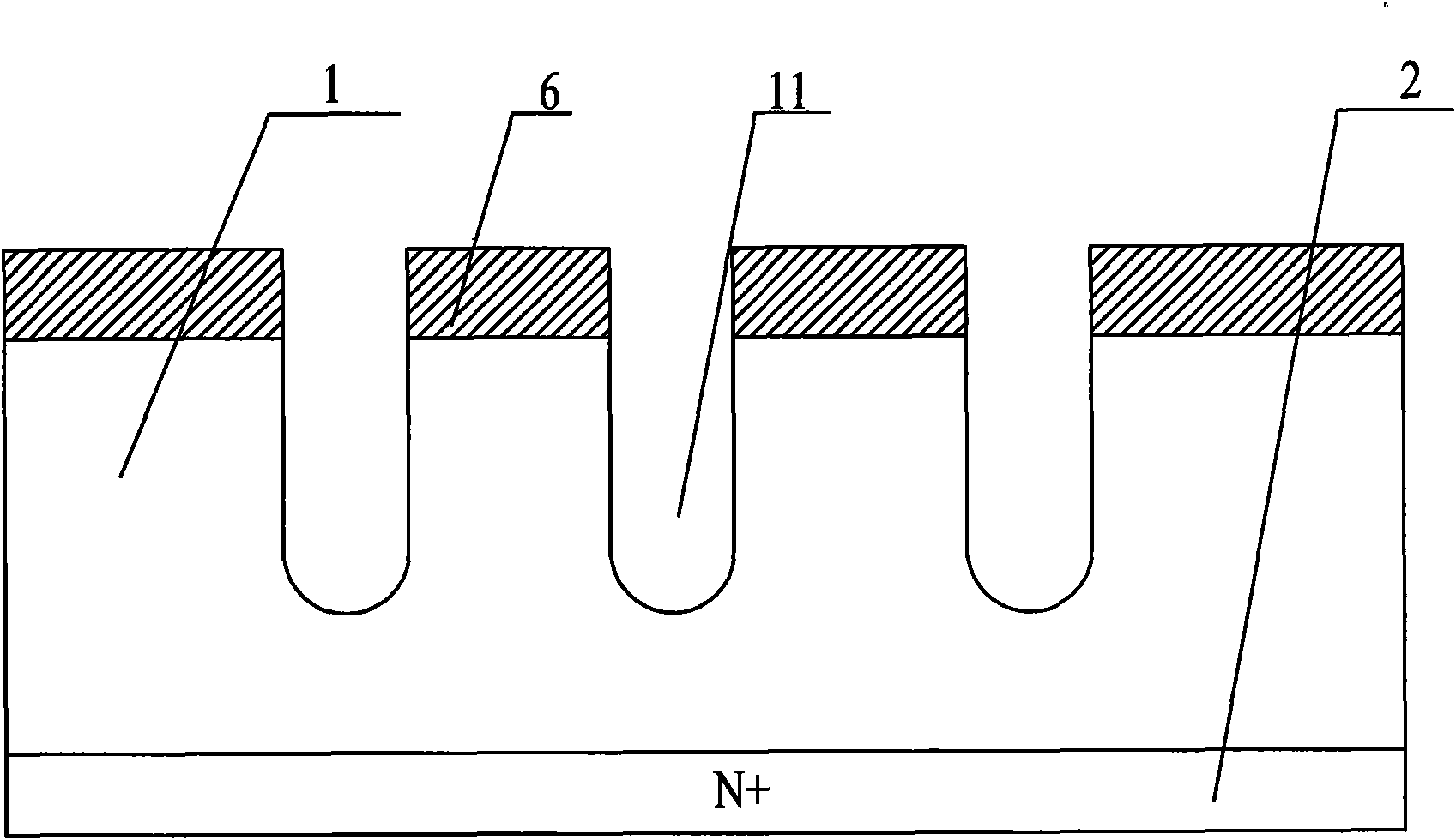
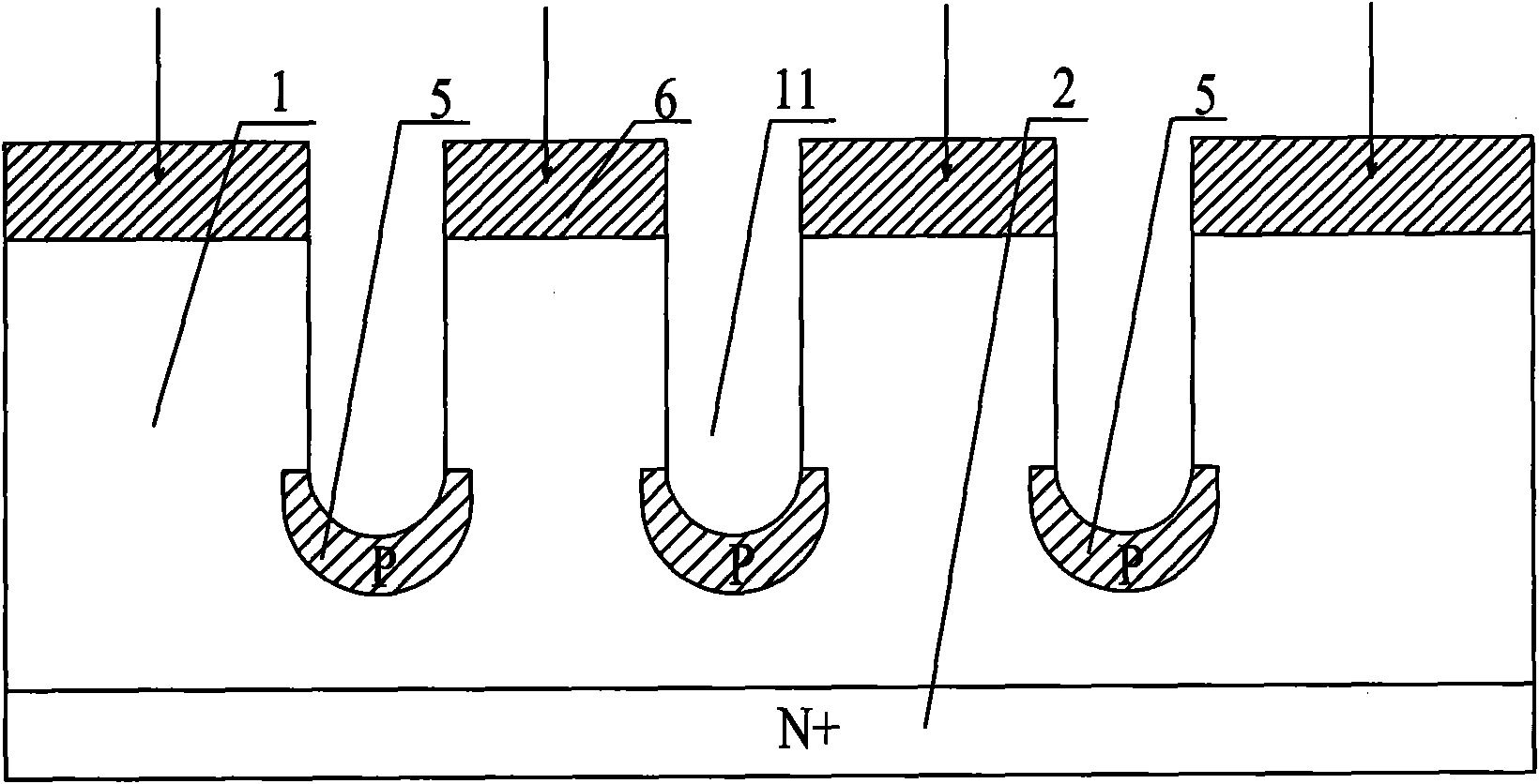
[0027] Such as Figure 1-7 As shown: taking an N-type semiconductor rectifier as an example, the present invention includes an N-type drift region 1, an N+ substrate 2, a second metal layer 3, a cathode terminal 4, a P-type surrounding layer 5, a hard mask layer 6, and an anode terminal 7 , a first metal layer 8 , an insulating oxide layer 9 , a first electrode 10 , a trench 11 , a mesa portion 12 and an N-type injection layer 13 .

[0028] Figure 7 It is a structural cross-sectional view of the trench type semiconductor rectifier. Such as Figure 7As shown: on the cross section of the semiconductor rectifier, the semiconductor rectifier includes a semiconductor substrate; the semiconductor substrate includes an N+ substrate 2 and an N-type drift region 1, the N-type drift region 1 is adjacent to the N+ substrate 2, and the N-type drift region The doping concentration of region 1 is lower than that of N+ substrate 2 . The semiconductor substrate has two opposite main surf...


PUM


Abstract

The invention relates to a grooved semiconductor rectifier and a manufacturing method thereof. The grooved semiconductor rectifier comprises a semiconductor baseplate, a first conduction type substrate and a first conduction type drift region, wherein one or more grooves extend from the first main plane to the first conduction type drift region, one or more mesa parts are limited at the upper part of the first conduction type drift region, and the upper part of the mesa part is provided with a first conduction type injection layer; the inner wall of the groove is covered with an insulation oxide layer, and a first electrode is deposited in the groove covered with the insulation oxide layer; the first conduction type drift region is provided with a second conduction type enclosure layer corresponding to the bottom of the groove, and the bottom of the groove is coated by the second conduction type enclosure layer; a first metal layer corresponding to the upper part of the first plane is deposited on the semiconductor baseplate; and the second plane of the semiconductor baseplate is covered with a second metal layer. The invention has the advantage of low manufacturing cost, and reduces the reverse leakage current and the forward conduction voltage drop of the Schottky rectifier.

Description

technical field [0001] The invention relates to a semiconductor rectifier and a manufacturing method thereof, in particular to a trench type semiconductor rectifier and a manufacturing method thereof. Background technique [0002] When a metal and a semiconductor are in contact, there is a contact potential difference because the work function of the metal is generally different from that of the semiconductor. As a result, a potential barrier is formed near the contact surface, which is usually called a Schottky barrier. Take the contact between metal and n-type semiconductor as an example. When metal and n-type semiconductor are in contact, electrons between the two materials will exchange to achieve a thermal balance, and finally make the Fermi level of the entire junction equal everywhere. Initially, electrons encounter a higher barrier to escape from metals than from semiconductors, so that, in reaching thermal equilibrium, there is a net flow of electrons from the semic...

Claims


Application Information

Patent Timeline
Patent Type & Authority Applications(China)
IPC IPC(8): H01L27/08H01L29/872H01L29/40H01L29/06H01L21/77H01L21/329
CPCH01L29/8725H01L29/0623H01L29/20H01L29/36H01L29/66143
Inventor 朱袁正叶鹏丁磊冷德武
Owner 无锡新洁能功率半导体有限公司
Why Eureka
Try Eureka