Semiconductor rectifying device and manufacturing method thereof

A manufacturing method and technology of rectifying devices, applied in semiconductor/solid-state device manufacturing, semiconductor devices, electric solid-state devices, etc., to achieve high reliability, reduce forward conduction voltage drop, and optimize source/drain contact areas

Inactive Publication Date: 2010-07-28
SUZHOU SILIKRON SEMICON CO LTD
View PDF1 Cites 7 Cited by
  • Summary
  • Abstract
  • Description
  • Claims
  • Application Information

AI Technical Summary

Problems solved by technology

[0004] The invention provides a method for manufacturing a semiconductor rectifier device with simple process and structure and high reliability and the resulting device. The technical problem to be solved is to overcome the problems of complex implementation of the existing process and poor reliability of the device

Method used


Image

  • Semiconductor rectifying device and manufacturing method thereof
  • Semiconductor rectifying device and manufacturing method thereof
  • Semiconductor rectifying device and manufacturing method thereof

Examples


Embodiment

[0044] Embodiment: A kind of manufacturing method of semiconductor rectifier device and obtained device

[0045] as attached Figure 1-9 Shown, a kind of manufacturing method of semiconductor rectifier device, the process is as follows:

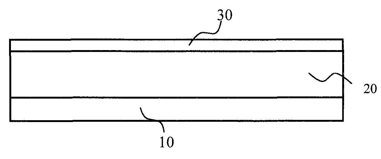
[0046] a) Provide a semiconductor substrate doped with N-type impurities with two opposite main surfaces, the semiconductor substrate consists of an N+ second main surface 10 as a silicon substrate and an N-first main surface 20 as an epitaxial layer composition;

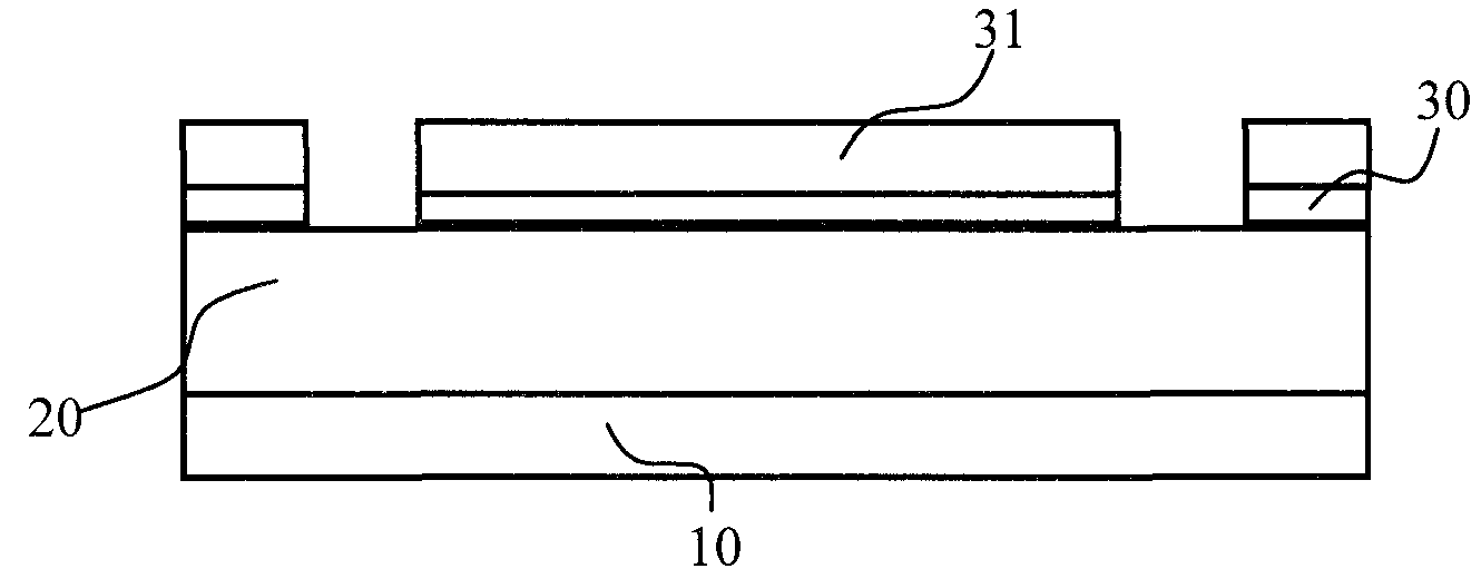
[0047] b) forming a field oxide layer 30 on the surface of the first main surface of the semiconductor substrate;

[0048] c) using a photoresist 31 to selectively cover the field oxide layer 30 to etch the field oxide layer in a part of the region;

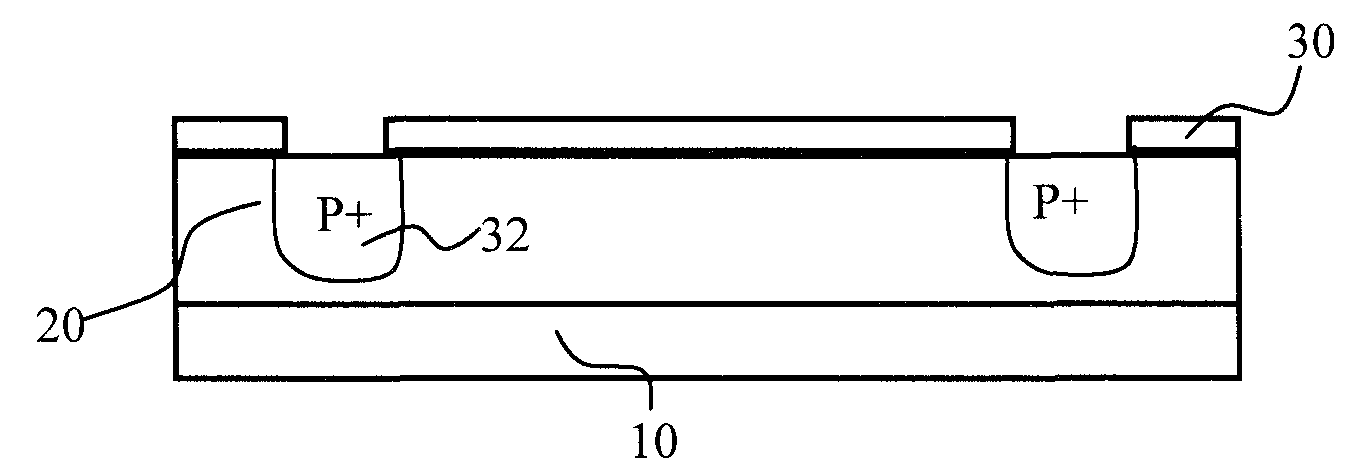
[0049] d) Remove the photoresist layer 31, use the field oxide layer 30 or the photoresist as a mask layer, inject P-type impurities into the N-first main surface, that is, the epitaxial layer 20, and then perform the thermal diffus...


PUM


Abstract

The invention discloses a semiconductor rectifying device and a manufacturing method thereof. The device is composed of an equivalent diode and a vertical MOS tube which are connected in parallel and comprises the following components: a) a semiconductor substrate with two relative major surfaces, which belongs to a first conduction type; wherein a first major surface is N-epitaxial layer and a second major surface is N+silicon base; b) a protective ring which is located on the first major surface for defining an active region, the protective ring is doped by a second conduction type; c) a gate oxide layer arranged below a polysilicon gate electrode; d) a second conduction type tagma is formed all round the gate oxide layer and on the epitaxial layer, a horizontal expansion region is arranged below the gate oxide layer, the horizontal expansion region serves as a channel region: e) an ohmic contact region of the second conduction type is formed on the surface of the tagma; in the invention, the problem that the existing technology is complex and reliability of device is poor is solved and a semiconductor rectifying device and a manufacturing method thereof featuring simple technology and high reliability are realized.

Description

technical field [0001] The invention relates to a manufacturing method and structure of a semiconductor rectifying device, in particular to a manufacturing method and structure of a power semiconductor rectifying device with a MOS structure. Background technique [0002] The Schottky diode is a majority carrier working device that utilizes the contact barrier between the metal and the semiconductor. It has the characteristics of low turn-on voltage, fast turn-off speed and unidirectional conduction. However, in order to make a Schottky diode, the Schottky contact barrier must be formed first; the formation of the Schottky barrier must use precious metals (gold, silver, platinum, molybdenum, nickel, etc.) as the anode, and the N-type silicon substrate is The cathode realizes its unidirectional conductivity through the barrier height difference between the metal and the silicon substrate. However, this manufacturing method requires the use of precious metals, is not compatibl...

Claims


Application Information

Patent Timeline
Patent Type & Authority Applications(China)
IPC IPC(8): H01L21/8249H01L27/06
Inventor 毛振东周名辉
Owner SUZHOU SILIKRON SEMICON CO LTD
Why Eureka
Try Eureka