Broad-spectrum absorption black silicon solar cell structure and preparation method thereof

A solar cell and manufacturing method technology, applied in circuits, photovoltaic power generation, electrical components, etc., can solve problems such as non-absorption, and achieve the effects of offsetting low mobility and current carrying, avoiding open circuit voltage, and increasing photogenerated current.

Inactive Publication Date: 2010-07-28
INST OF SEMICONDUCTORS - CHINESE ACAD OF SCI
View PDF0 Cites 34 Cited by
  • Summary
  • Abstract
  • Description
  • Claims
  • Application Information

AI Technical Summary

Problems solved by technology

[0007] In view of this, the main purpose of the present invention is to propose a broad-spectrum absorption black silicon solar cell structure and its manufacturing method to solve the problem that traditional silicon

Method used


Image

  • Broad-spectrum absorption black silicon solar cell structure and preparation method thereof
  • Broad-spectrum absorption black silicon solar cell structure and preparation method thereof
  • Broad-spectrum absorption black silicon solar cell structure and preparation method thereof

Examples


Example Embodiment

[0040] In order to make the objectives, technical solutions, and advantages of the present invention clearer, the following further describes the present invention in detail in conjunction with specific embodiments and with reference to the accompanying drawings.
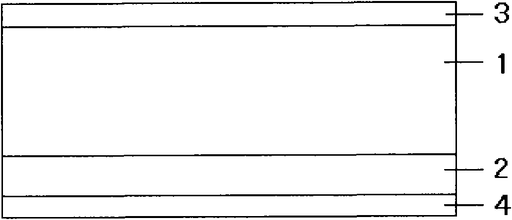
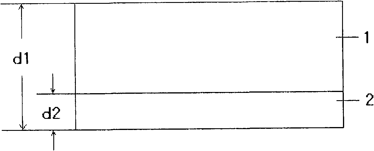
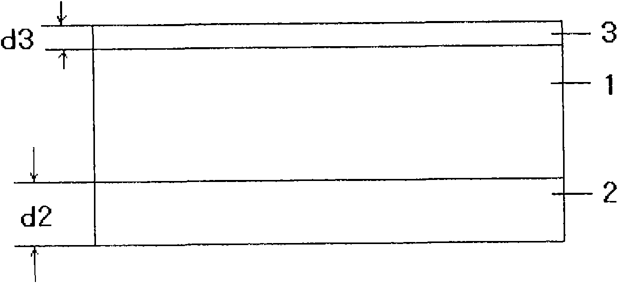
[0041] The broad-spectrum absorbing black silicon solar cell structure provided by the present invention absorbs the penetrating infrared light through the black silicon layer on the back, and uses the impurity gradient field to separate the photogenerated electron-hole pairs generated therein and convert them into photocurrent. It solves the limitation that traditional silicon-based solar cells cannot absorb and convert the near-infrared solar spectrum with wavelengths above 1.1 microns, and can effectively improve the photoelectric conversion efficiency of silicon-based solar cells.

[0042] Such as figure 1 As shown, figure 1 It is a schematic diagram of the broad-spectrum absorption black silicon solar cell structure ...


PUM

PropertyMeasurementUnit
Intervalaaaaaaaaaa
Scaleaaaaaaaaaa
Depthaaaaaaaaaa

Abstract

The invention discloses a broad-spectrum absorption black silicon solar cell structure. The structure sequentially comprises an irradiated face broad spectrum light trapping layer, a p-shaped silicon substrate, a n-shaped phosphorous diffusion layer and a backlight surface broad-spectrum absorption black silicon layer from top to bottom. The invention simutaneously discloses a preparation method of the broad-spectrum absorption black silicon solar cell structure. In the invention, the characteristics of the black silicon material can be fully utilized to enable sunlights entering into the cell to be almost absorbed; simutaneously a back dopant gradient can be utilized to separate eletron-hole pairs generated in the black silicon by a self-configuration field separation method, so that the eletron-hole pairs can be received and transfomred into light current by electrodes, thereby solving the problem that the traditional silicon substrate cell can not absorb and transform solar spectrum of which the wavelength is above 1.1 microns; and the PN junction of the structure is formed by diffuse junctions, the open-circuit voltage of the cell can be ensured not to be influenced by lowered black silicon lower-energy photon conversion, thereby effectively improving the photoelectric conversion efficiency of the silicon substrate sollar cell.

Description

technical field [0001] The invention relates to the technical field of silicon-based solar cells, in particular to a broad-spectrum absorption black silicon solar cell structure and a manufacturing method thereof. Background technique [0002] Solar energy is an inexhaustible, non-polluting, renewable and clean energy with the greatest potential for development. The silicon material abundant on the earth is the best material for making solar cells. However, the cost of power generation of silicon-based cells is still relatively high at present. It is difficult to popularize civilian use. An important way to reduce the price of electricity generated by silicon-based solar cells is to improve the photoelectric conversion efficiency of the cells. The main technical means currently used are to reduce the reflectivity of light on the surface of the battery, such as the use of transparent anti-reflection electrode film, pyramid textured surface, porous silicon light-trapping surf...

Claims


Application Information

Patent Timeline
IPC IPC(8): H01L31/068H01L31/18H01L31/0236
CPCY02E10/50Y02E10/547Y02P70/50
Inventor 朱洪亮朱小宁梁松张兴旺刘德伟王圩
Owner INST OF SEMICONDUCTORS - CHINESE ACAD OF SCI
Why Eureka
Try Eureka