Low-power consumption micro-heater with mesh-structured heating film and fabrication method thereof
A heating film and heater technology, applied in the direction of microstructure technology, microstructure devices, ohmic resistance heating, etc., can solve the problems of affecting sensor sensitivity and low catalyst coverage, increase the corrosion window area, facilitate arraying and batch production Production, the effect of reducing the release time
- Summary
- Abstract
- Description
- Claims
- Application Information
AI Technical Summary
Problems solved by technology
Method used
Image
Examples
Embodiment 1
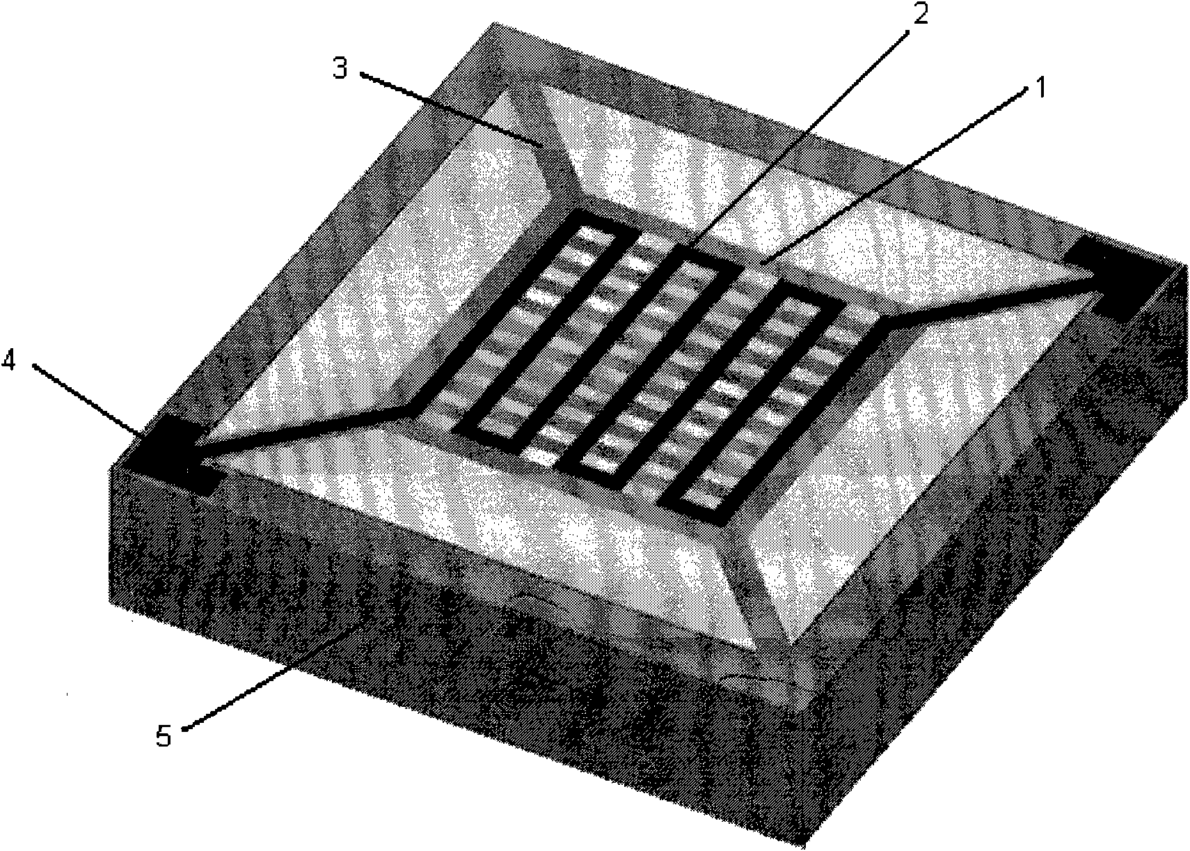
[0033] The micro-heater structure described in this embodiment can be found in figure 1 . Its production process is as follows:
[0034]1. Fabricate a dielectric film on a silicon wafer. Select an N-type (100) silicon wafer, first thermally oxidize and grow silicon oxide with a thickness of 0-3 microns, then use LPCVD to deposit silicon nitride with a thickness of 0.5 microns on the silicon wafer, and then use PECVD to deposit a thickness of 0.5 microns on the front side of the silicon wafer. 0.2 micron silicon oxide.
[0035] 2. Make heating resistance wire. The pattern of the heating resistance wire and electrode is photo-etched on the front side, and the metal Ti / Pt is sputtered with a thickness of 0.01 / 0.3 microns, and then the single-fold heating resistance wire and the electrode for the lead are produced by using the lift-off (lift-off) process, and then heated in nitrogen Annealed at 350°C for half an hour under atmosphere.
[0036] 3. Fabricate a heating film with...
Embodiment 2
[0039] The top view of the front structure of the micro-heater described in this embodiment can be found in Figure 7 . Its production process is as follows:
[0040] 1. Fabricate a dielectric film on a silicon wafer. Select a P-type (100) silicon wafer, first thermally oxidize and grow silicon oxide with a thickness of 0.5 micron, and then use LPCVD to deposit silicon nitride with a thickness of 1 micron on the silicon wafer.
[0041] 2. Make heating resistance wire. First sputter metal Ti / Au with a thickness of about 0.01 / 0.2 microns, then pattern photolithography, use gold corrosion solution and titanium corrosion solution to make single-line heating resistance wires and electrodes for leads, and finally in a nitrogen atmosphere at 350 ℃ for half an hour.
[0042] 3. Fabricate a heating film with a mesh structure and support cantilever beams. Front photolithography, under the protection of photoresist, use RIE to dry-etch the composite film of silicon oxide and silicon...
Embodiment 3
[0045] The top view of the front structure of the micro-heater described in this embodiment can be found in Figure 8 . Its production process is as follows:
[0046] 1. Fabricate a dielectric film on a silicon wafer. An N-type (110) silicon wafer is selected, and silicon oxide with a thickness of 0.5 microns is deposited by LPCVD.
[0047] 2. Make heating resistance wire. First sputter the metal seed layer of titanium and platinum, then define two parallel bifold heating resistance wires and lead electrodes by photolithography, electroplate a layer of metal platinum with a thickness of 1 micron, and finally remove the photoresist and seed layer, And annealed at 350°C for half an hour under nitrogen atmosphere.
[0048] 3. Fabricate a heating film with a mesh structure and support cantilever beams. Front photolithography, under the protection of photoresist, use RIE to dry etch the silicon oxide film until the substrate silicon is exposed, and the etched place forms a mes...
PUM
| Property | Measurement | Unit |
|---|---|---|
| Thickness | aaaaa | aaaaa |
| Thickness | aaaaa | aaaaa |
Abstract
Description
Claims
Application Information


