Novel super-hard TiB2/c-BN nano multi-layer film prepared by magnetron sputtering technique
A nano-multi-layer and multi-layer film technology, which is applied in the direction of sputtering plating, coating, layered products, etc., can solve the problems of high melting point, small friction coefficient, high chemical stability, etc., to improve wear resistance, Effects of improving friction performance and improving production efficiency
- Summary
- Abstract
- Description
- Claims
- Application Information
AI Technical Summary
Problems solved by technology
Method used
Image
Examples
Embodiment 1
[0043] Synthesis of TiB by Changing Modulation Ratio Combined with Substrate Heating Conditions 2 / c-BN nano multilayer film:
[0044] (1) Before the experiment, use acetone and absolute alcohol to treat Al 2 o 3 The slices were ultrasonically cleaned for 15 min, dried and then put into the magnetron sputtering coating chamber.
[0045] (2) Vacuum the chamber so that the background vacuum in the chamber is 2.0×10 -4 Pa~3.8×10 -4 Pa.
[0046] (3) Adjust the flapper valve so that the working air pressure is 6Pa. Use a mass flow meter to control the Ar intake flow to keep it at 80sccm. Turn on the bias power supply and adjust the base bias voltage -80V. The current is normal, and use Ar The ion-pair sample is bombarded and cleaned for at least 5 minutes, the bias power is turned off, and the flapper valve is adjusted to make the working air pressure 3Pa.
[0047] (4) Turn on the 500W radio frequency power supply, control the Ar intake flow rate with a mass flow meter to kee...
Embodiment 2
[0052] Synthesis of TiB under changing modulation ratio combined with substrate heating 2 / BN nano multilayer film:
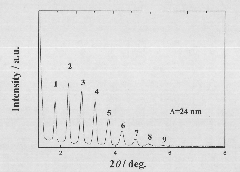
[0053] Deposition parameters: substrate temperature controlled at 225°C, heating current 2.8A; modulation ratio 13:1 (TiB 2 : h-BN), the modulation modulation period is 24nm; the multilayer film is prepared from 25 to 32 layers, the Ar flow: 40 to 45 sccm; the background vacuum degree: 2.0×10 -4 Pa~3.8×10 -4 Pa; working pressure: 0.2Pa; RF sputtering source process parameters: RF target TiB 2 The sputtering power is 90W, and the h-BN sputtering power is 200W; the target base distance is 6cm, and the base bias voltage is -80V. The thickness of the Ti transition layer is 65nm, and the deposition time is controlled at about 1200s.
[0054] For the optimal conditions, the preparatory work before the experiment is as described in (1)-(5) above. From the modulation layer thickness and modulation ratio, the single-layer TiB 2 Thickness is 22.3nm, BN thickness is ...
Embodiment 3
[0056] in Al 2 o 3 (111) Deposit 40nm TiB on the substrate 2 As a transition layer, alternately deposit h-BN and TiB 2 As a multilayer film, the layer thickness per modulation period is 20nm, the modulation period of the multilayer film is 28 layers, and the total layer thickness is 500nm; where h-BN:TiB 2 The modulation ratio is 1:3.
[0057] For the optimal conditions, the preparatory work before the experiment is as described in (1)-(5) above. From the modulation layer thickness and modulation ratio, the single-layer TiB 2 Thickness is 22.3nm, BN thickness is 1.7nm, then according to TiB 2 And the deposition rate of BN, calculate their sputtering time. Set 25 modulation cycles back and forth between the two targets. The substrate temperature was maintained at 225°C. This way you can get the required TiB 2 / c-BN nano multilayer film
PUM
| Property | Measurement | Unit |
|---|---|---|
| hardness | aaaaa | aaaaa |
| elastic modulus | aaaaa | aaaaa |
| thickness | aaaaa | aaaaa |
Abstract
Description
Claims
Application Information


