Ultrahard TiB2/Si3N4 nano-multilayer film and preparation method thereof

A nano-multi-layer and multi-layer film technology, applied in coatings, layered products, metal material coating processes, etc., can solve problems such as low hardness, high brittleness, and poor bonding between the film and the substrate

Inactive Publication Date: 2012-04-25
TIANJIN NORMAL UNIVERSITY
View PDF0 Cites 0 Cited by
  • Summary
  • Abstract
  • Description
  • Claims
  • Application Information

AI Technical Summary

Problems solved by technology

At the same time, it is necessary to solve the problem of synthesizing TiB 2 and Si 3 N 4 Technical problems such as low hardness, high brittleness, and poor bonding between the film and the substrate exist in the film

Method used


Image

  • Ultrahard TiB2/Si3N4 nano-multilayer film and preparation method thereof
  • Ultrahard TiB2/Si3N4 nano-multilayer film and preparation method thereof
  • Ultrahard TiB2/Si3N4 nano-multilayer film and preparation method thereof

Examples


Embodiment 1

[0077] Synthetic process parameters: Before the experiment, the Si wafer was ultrasonically cleaned with acetone and absolute alcohol for 15 minutes, dried and put into the ion beam assisted deposition coating chamber. The sputtering gas used in the deposition process is pure Ar 2 , use a mass flow controller to control the flow rate at 4.02 ml / s; background vacuum: 1.9×10⁻⁴Pa~2.0×10⁻⁴Pa, working pressure between 1.2×10⁻²Pa~1.3×10⁻²Pa; splash Sputtering ion source process parameters: discharge voltage 70V, acceleration voltage 200V, sputtering energy 1.05keV, sputtering beam current 25mA. with low energy Ar + When the ion gun is cleaned, its process parameters: discharge voltage 70V, acceleration voltage 100V, auxiliary energy 200eV, auxiliary beam current 5mA; substrate heating temperature: 25-425°C.

[0078] Preparation process: first deposit Ti as a transition layer on a single-sided polished Si(100) substrate, and then alternately deposit TiB 2 and Si 3 N 4 Do multi-l...

Embodiment 2

[0080] TiB 2 / Si 3 N 4 Synthesis of nano-multilayer films:

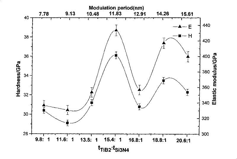
[0081] Control substrate heating temperature 225°C, modulation period 9nm, modulation ratio Si 3 N 4 :TiB 2 1:9 (equivalent to TiB 2 8.1nm thick, Si 3 N 4 The thickness of the transition layer is 0.9nm), the thickness of the transition layer is 30nm, the Ar gas flow is maintained at 4.02sccm; the sputtering energy is 1.05keV; the sputtering beam is 25mA, where TiB 2 and Si 3 N 4 The sputtering energy is 1.05keV; the sputtering beam current is 25mA; the heating current is 2-2.8A. The total working air pressure is 1.2-1.3×10 -2 Pa. There are 60 cycles between the two targets, and the computer program precisely controls TiB 2 with Si 3 N 4 The sputtering time is 300 seconds and 50 seconds. The total thickness of the film is about 450 nm. The film is in the high vacuum chamber, and the chamber is not opened until the temperature drops to room temperature. The preparation process is the same as in Examp...

Embodiment 3

[0083] TiB 2 / Si 3 N 4 Synthesis of nano-multilayer films:

[0084] TiB 2 Thickness 11.21nm, Si 3 N 4 The thickness is 0.79nm, 11.8m (equivalent to the modulation ratio Si 3 N 4 :TiB 2 =1:15.6), the substrate temperature was kept at 225°C. There are 34-51 cycles between the two targets. The total working air pressure is 1.2-1.3×10 -2 Pa. Computer program precisely controls TiB 2 with Si 3 N 4 The sputtering time is 410 seconds and 40 seconds. where TiB 2 and Si 3 N 4 The sputtering energy is 1.05keV; the sputtering beam current is 25mA; the heating current is 2-2.8A. The total thickness of the film is about 600 nm. The film is in the high vacuum chamber, and the chamber is not opened until the temperature drops to room temperature to obtain TiB 2 / Si 3 N 4 Nano multilayer film. The preparation process is the same as in Example 1.


PUM

PropertyMeasurementUnit
thicknessaaaaaaaaaa
thicknessaaaaaaaaaa
hardnessaaaaaaaaaa

Abstract

The invention relates to an ultrahard TiB2 / Si3N4 nano-multilayer film and a preparation method thereof. The ultrahard TiB2 / Si3N4 nano-multilayer film is to alternately deposit a TiB2 layer and a Si3N4 layer on a pure Ti transition layer with a thickness of 0-60nm; wherein the modulation ratio between the TiB2 layer and the Si3N4 layer is 3-20.6:1; the thickness of the layer is 3-15nm at each period, the periodic numbers of the multilayer film are 27-200 layers, and the thickness of the nano-multilayer film is 400-600nm. The novel ultrahard TiB2 / Si3N4 nano-multilayer film has not only excellent high temperature oxidation resistance but also high rigidity up to 36.2 GPa, lower internal stress (2.5GPa) and higher film and substrate bonding strength (about 62.579mN). The TiB2 / Si3N4 nano-multilayer film of the invention has very high application value as a coating of a high speed cutting tool and other wear-resistant workpieces served therewith at high temperature.

Description

technical field [0001] The invention belongs to the technical field of surface strengthening film treatment of various cutting tools and moulds. involving superhard TiB 2 / Si 3 N 4 Nano multilayer film and its preparation method. More specifically, it is a superhard TiB prepared by high vacuum ion beam assisted deposition system (IBAD). 2 / Si 3 N 4 The method of nano-multilayer film. Background technique [0002] Boride ceramics are a class of ceramics with special physical and chemical properties. Because of its extremely high melting point, high chemical stability, high hardness and excellent wear resistance, it is used as hard tool materials, abrasives, alloy additives and wear-resistant parts, etc. At the same time, this type of material has excellent electrical properties. It can be used as an inert electrode material and a high-temperature electrical material to attract attention. In recent decades, countries all over the world are stepping up the research and...

Claims


Application Information

Patent Timeline
Patent Type & Authority Patents(China)
IPC IPC(8): B32B9/00B32B7/02C23C14/34C23C14/06C23C14/54
Inventor 李德军董磊曹猛邓湘云
Owner TIANJIN NORMAL UNIVERSITY
Why Eureka
Try Eureka