

Method for preparing epitaxial growing nano pattern substrate of nitride
A nano-patterning and epitaxial growth technology, applied in electrical components, circuits, semiconductor devices, etc., can solve the problems of limited brightness improvement, complex process, expensive equipment, etc., to relax stress, reduce dislocation density, and improve performance. Effect
Inactive Publication Date: 2010-08-25
EPILIGHT TECH
View PDF6 Cites 11 Cited by
- Summary
- Abstract
- Description
- Claims
- Application Information
AI Technical Summary
Problems solved by technology
However, at present, this kind of pattern is on the micron scale, which has limited improvement in brightness; compared with the usual micron-scale patterned substrate, the nano-patterned substrate technology can more effectively relax the stress of the growth process of the heterojunction interface, Further reduce the dislocation density of the nitride epitaxial layer, improve the crystal quality of the material and the corresponding device performance
The realization of semiconductor nanoscale patterns usually adopts electron beam lithography or X-ray lithography, but these lithography techniques involve expensive equipment, complicated process and high cost.
Method used
View moreImage
Smart ImageViewing Examples

Examples
Embodiment Construction
Login to View More PUM
| Property | Measurement | Unit |
|---|---|---|
| diameter | aaaaa | aaaaa |
| diameter | aaaaa | aaaaa |
| thickness | aaaaa | aaaaa |
Abstract
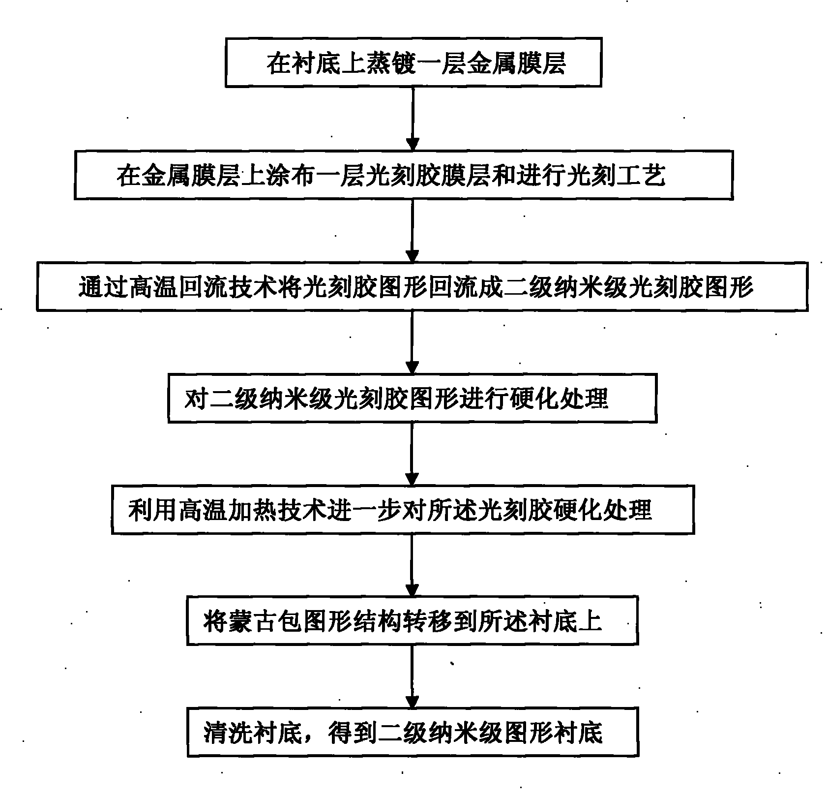
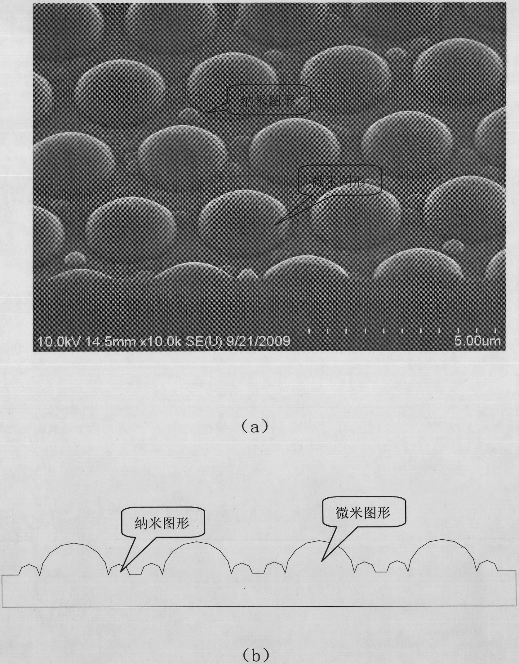
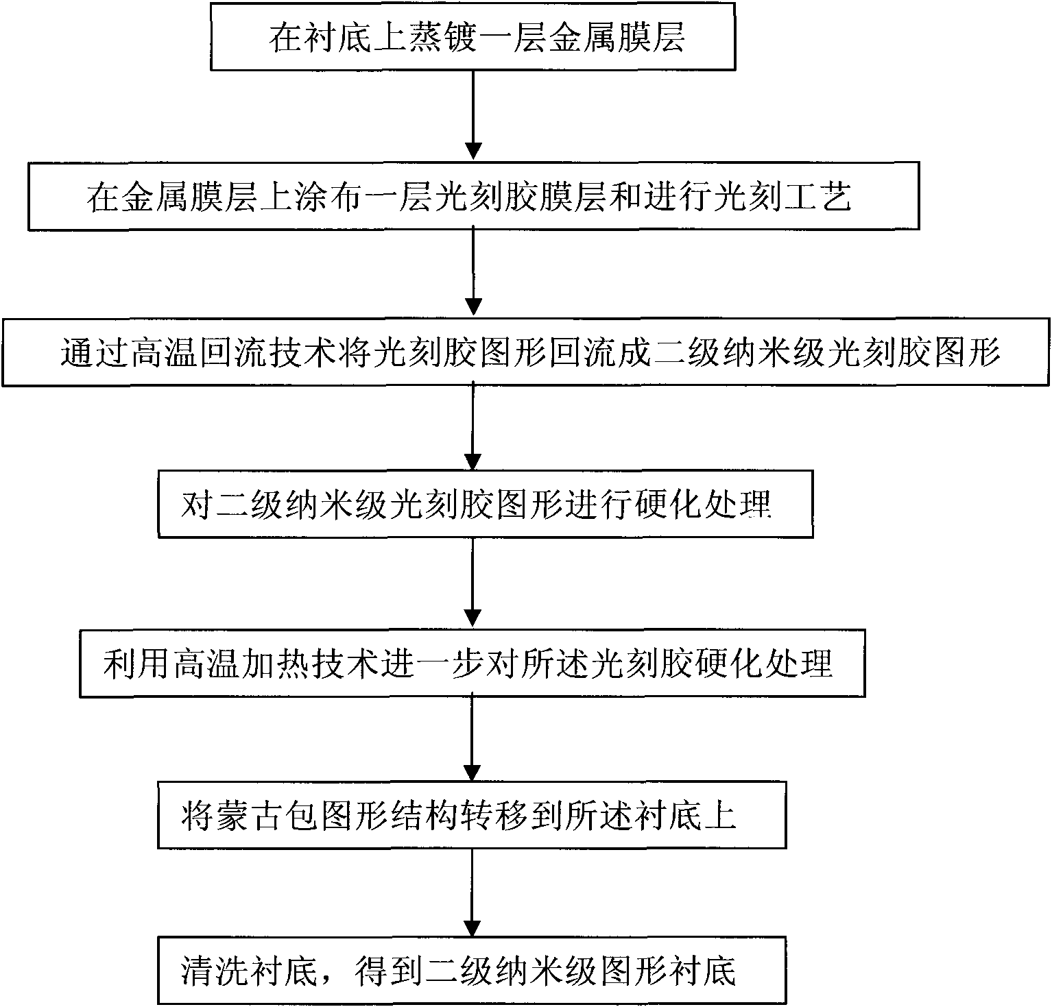
The invention discloses a method for preparing an epitaxial growing nano pattern substrate of a nitride, which comprises the following steps of: evaporating a metal film layer on a substrate; coating a photoresist film layer on the metal film layer; developing nano-size photoresist patterns on the substrate by a photomask technology and retaining a layer of thin photoresist between the patterns; forming two stages of nano-grade photoresist patterns by a high-temperature reflux technology, wherein one stage of nano-grade photoresist pattern is a micron-size pattern, and the other stage of nano-grade photoresist pattern is a nano-size pattern; carrying out hardening processing on the two stages of nano-grade photoresist patterns; further hardening the photoresist patterns by utilizing a photoresist heating and baking technology; transferring the photoresist pattern structures on the substrate by utilizing the two formed stages of nano-grade photoresist patterns as mask films through a dry etching technology; and cleaning the substrate to obtain two stages of nano-grade pattern substrates. The invention can improve the crystal quality of materials and the corresponding device performance.
Description
Preparation method of nano-pattern substrate for nitride epitaxial growth technical field The invention relates to the field of semiconductor light-emitting diodes, in particular to a method for preparing a nitride epitaxy-grown nano-pattern substrate. Background technique Light-emitting diodes have the advantages of small size, high efficiency and long life, and are widely used in traffic indication, outdoor full-color display and other fields. In particular, the use of high-power light-emitting diodes may realize semiconductor solid-state lighting, which has caused a revolution in the history of human lighting, and has gradually become a research hotspot in the field of electronics. In order to obtain high-brightness LEDs, the key is to improve the internal quantum efficiency and external quantum efficiency of the device. At present, the light extraction efficiency of the chip is the main factor limiting the external quantum efficiency of the device. The main reason is ...
Claims
Login to View More Application Information
Patent Timeline
 Patent Type & AuthorityApplications(China)
IPC IPC(8): H01L33/12
Inventor袁根如郝茂盛陈诚
OwnerEPILIGHT TECH