Low-loss microstrip patch frequency scanning antenna array capable of scanning by large angle in limited bandwidth

A microstrip patch, limited bandwidth technology, applied in the field of frequency scanning antenna arrays, can solve the problems of increased loss, limited scanning angle, large loss, etc., to achieve the effect of simple structure, improved performance, and reduced loss

Inactive Publication Date: 2010-08-25
NANJING UNIV OF SCI & TECH
View PDF5 Cites 33 Cited by
  • Summary
  • Abstract
  • Description
  • Claims
  • Application Information

AI Technical Summary

Problems solved by technology

But their volume and weight are relatively large, and the profile is relatively high, thus limiting their application range
Since the end of the 1970s, microstrip antenna arrays with beam scanning capabilities have been proposed one after another, which are mainly divided into two categories. One is to use the leaky wave mode for frequency scanning. The leaky wave antenna has a simple structure and high efficiency, but the scanning angle It is limited and cannot achieve wide-angle scanning; the other is to use microstrip slow wave lines for scanning, but the loss of microstrip lines is large, which limits th

Method used


Image

  • Low-loss microstrip patch frequency scanning antenna array capable of scanning by large angle in limited bandwidth
  • Low-loss microstrip patch frequency scanning antenna array capable of scanning by large angle in limited bandwidth
  • Low-loss microstrip patch frequency scanning antenna array capable of scanning by large angle in limited bandwidth

Examples


Embodiment

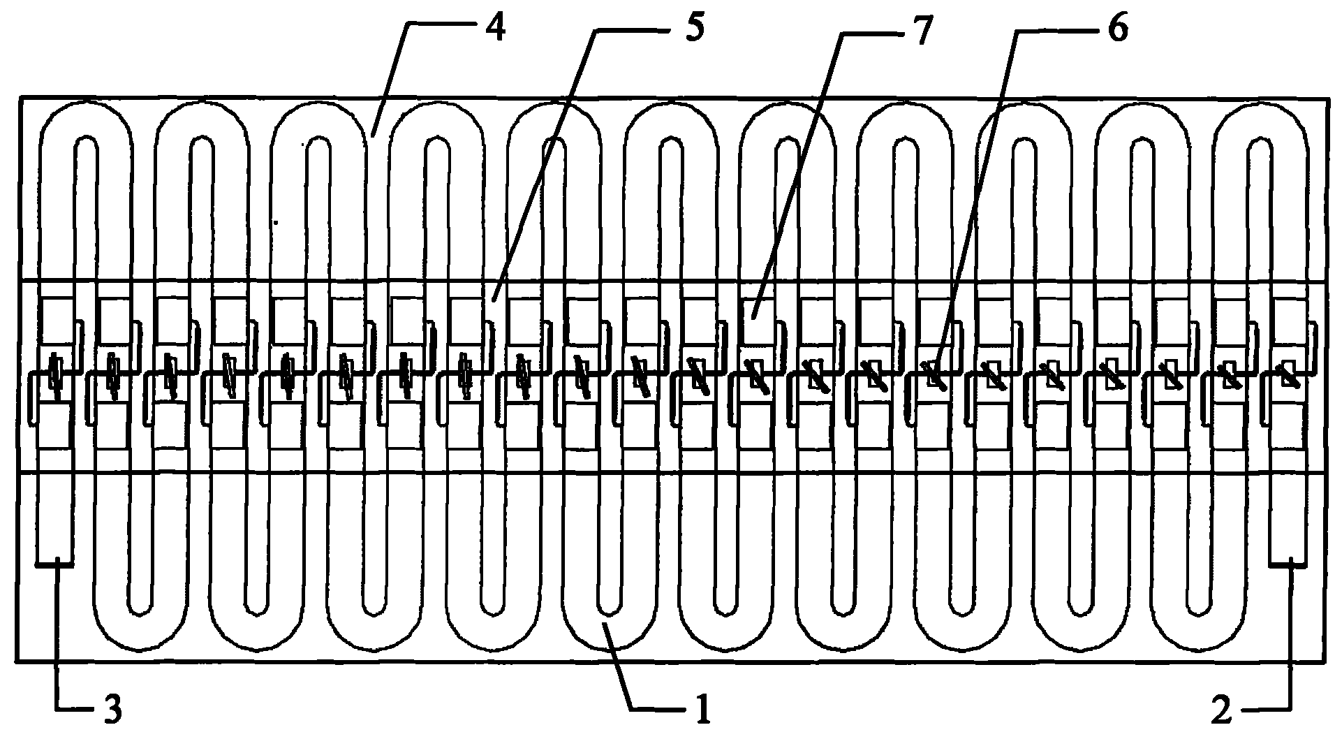
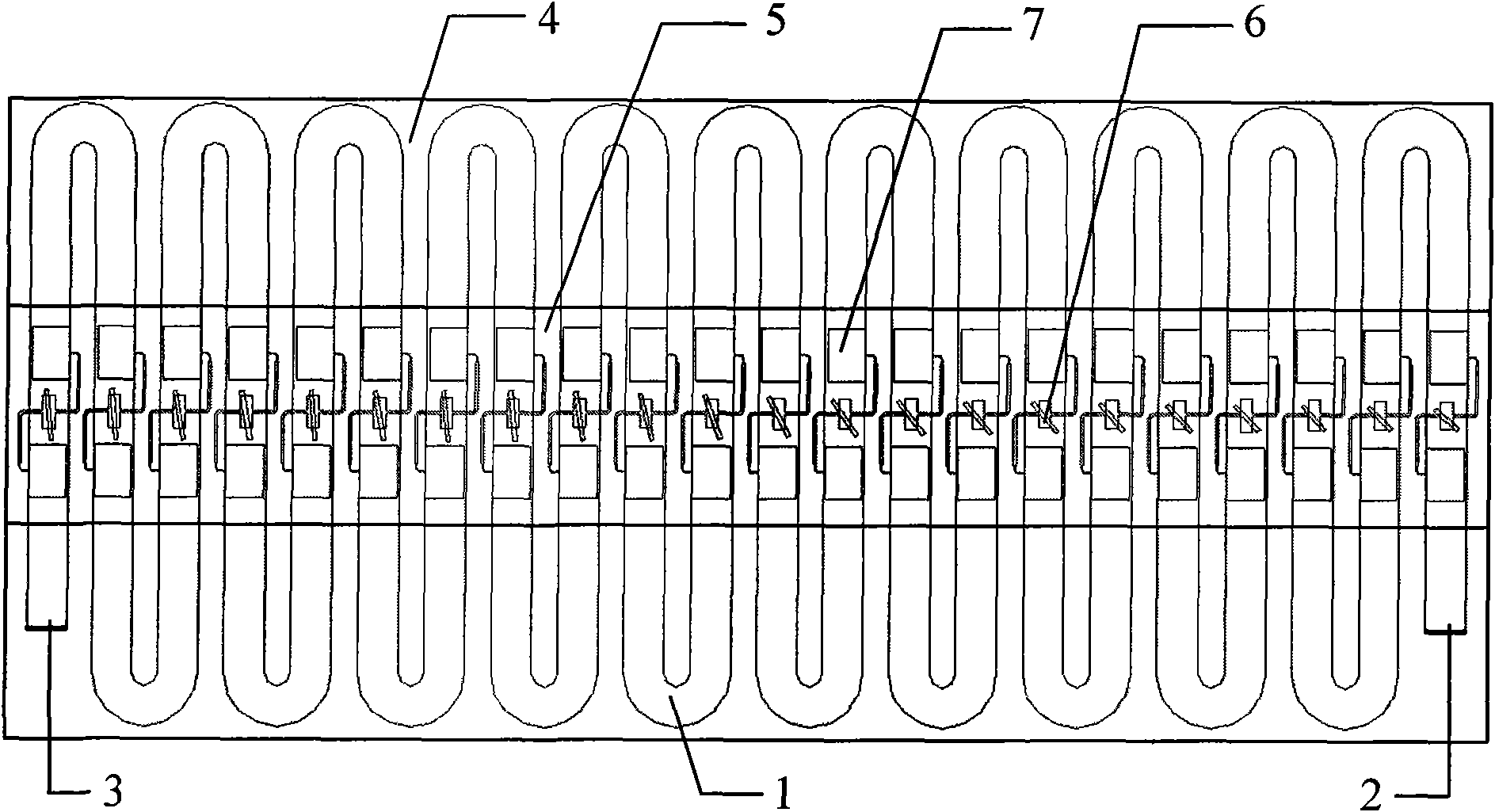
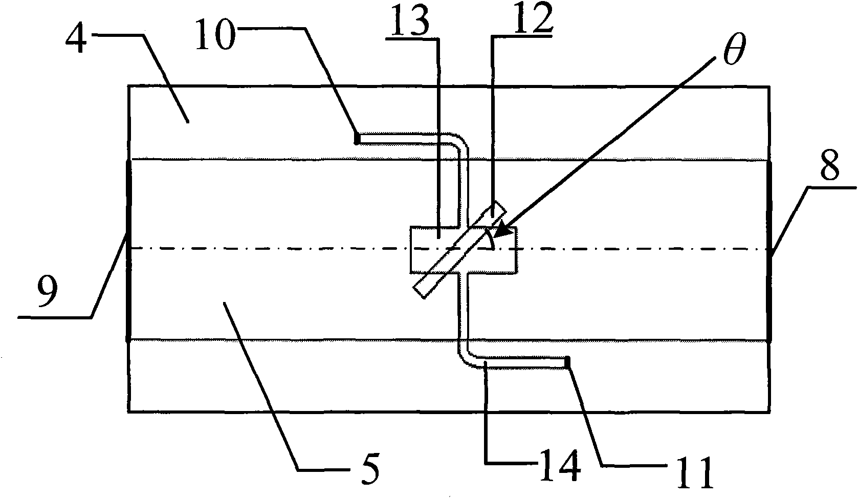
[0019] Figure 2 is a waveguide slot microstrip patch hybrid feed network, which is a component of the low-loss microstrip patch frequency-swept antenna array scanned from a large angle within the limited bandwidth in Figure 1, consisting of a metal floor 4, a dielectric substrate 5, Waveguide ports 8, 9, microstrip line ports 10, 11, oblique rectangular slot 12, coupling microstrip patch 13, microstrip transmission line 14, waveguide ports 8, 9 are connected with curved waveguide slow wave lines before and after, microstrip The wire ports 10 , 11 are connected to the microstrip patch unit 7 . The E-plane curved waveguide 1 is placed at the bottom of the array, and the metal floor 4 provided with rectangular slots 12 is placed on the E-plane curved waveguide 1 and connected together. A dielectric substrate 5 is provided on the metal floor 4, a coupling microstrip patch 13 is provided on the dielectric substrate 5 at a position corresponding to each slit 12, and a microstrip tra...


PUM

PropertyMeasurementUnit
Slopeaaaaaaaaaa
Widthaaaaaaaaaa
Lengthaaaaaaaaaa

Abstract

The invention discloses a low-loss microstrip patch frequency scanning antenna array capable of scanning by a large angle in a limited bandwidth. The low-loss microstrip patch frequency scanning antenna array comprises an E-plane bend waveguide, a metal floor, a medium base plate, a waveguide gap microstrip patch mixed feeding structure and microstrip patch units, wherein one end of the E-plane bend waveguide is provided with a feeding port, and the other end of the E-plane bend waveguide is provided with a waveguide port which is connected with matched load; the metal floor is arranged on the E-plane bend waveguide; rectangular gaps are formed on the metal floor; the medium base plate is arranged on the metal floor; two rows of the microstrip patch units are arranged on the medium base plate; the number of each row of the microstrip patch units is as same as that of the gaps; all the microstrip patch units form the microstrip patch antenna array; a coupling microstrip patch is arranged on the medium base plate corresponding to each gap, on the medium base plate; microstrip transmission lines are symmetrically connected with the two sides of each coupling microstrip patch respectively; and the ports of the microstrip transmission lines are connected with the corresponding microstrip patch units respectively. The low-loss microstrip patch frequency scanning antenna array has the advantages of obviously reducing the loss of a frequency scanning slow wave line and improving the performance of the frequency scanning antenna.

Description

technical field [0001] The invention belongs to a frequency-scanning antenna array, in particular to a low-loss microstrip patch frequency-scanning antenna array for large-angle scanning within a limited bandwidth. Background technique [0002] Electronic scanning antenna overcomes the shortcomings of slow scanning speed in traditional mechanical scanning, and has been widely used in military and civilian fields such as radar, communication, and mobile TV, and has developed rapidly. There are four main types of antenna electronic scanning techniques: phase scanning, frequency scanning, time delay scanning and electronic feed switch scanning. Among them, phase sweep and frequency sweep are the most used. Phase scanning is to realize beam scanning by changing the phase of the input signal of the array elements; frequency scanning is to change the "intra-array phase difference" between antenna elements by changing the signal frequency, so as to realize beam scanning. In addit...

Claims


Application Information

Patent Timeline
IPC IPC(8): H01Q3/34H01Q21/00H01Q13/08H01Q13/10H01Q1/48
Inventor 王昊葛平马晓峰盛卫星
Owner NANJING UNIV OF SCI & TECH
Why Eureka
Try Eureka