
P type lateral insulated gate bipolar device for reducing hot carrier effect

A technology of bipolar devices and hot carriers, applied in the direction of semiconductor devices, electrical components, circuits, etc., can solve problems affecting the service life of devices, prolong the degradation life, fully compatible with the integrated circuit manufacturing process, and reduce ion generation rate effect

Inactive Publication Date: 2010-09-01
SOUTHEAST UNIV
View PDF3 Cites 8 Cited by
  • Summary
  • Abstract
  • Description
  • Claims
  • Application Information

AI Technical Summary

Problems solved by technology

In addition, because power semiconductor devices work at very high voltages, the hot carrier effect will cause the performance parameters of the device such as threshold voltage, on-resistance, and gain to degrade to varying degrees with the increase of use time, seriously affecting the device. service life

Method used


Image

  • P type lateral insulated gate bipolar device for reducing hot carrier effect
  • P type lateral insulated gate bipolar device for reducing hot carrier effect
  • P type lateral insulated gate bipolar device for reducing hot carrier effect

Examples


Embodiment Construction

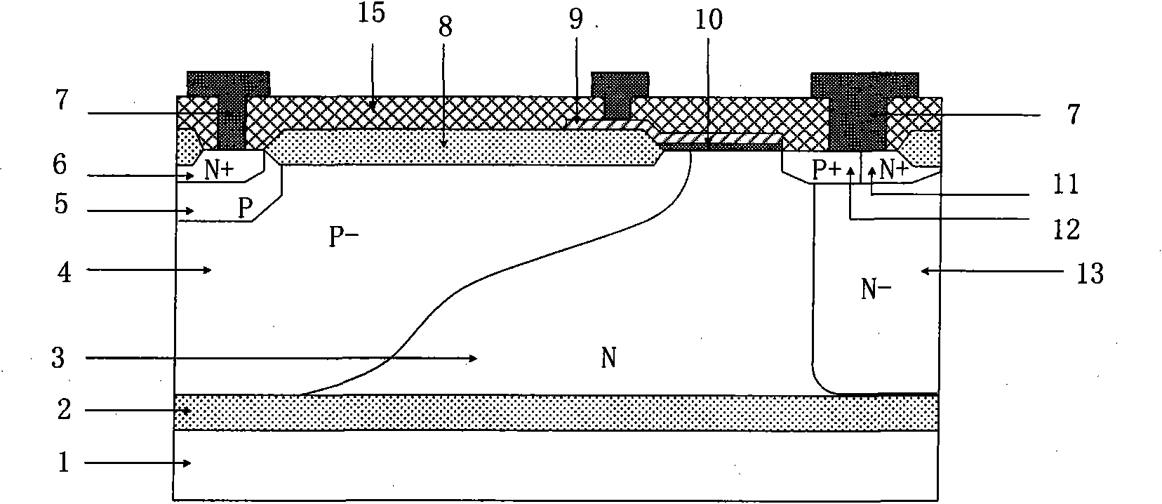
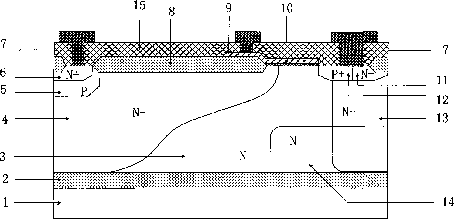
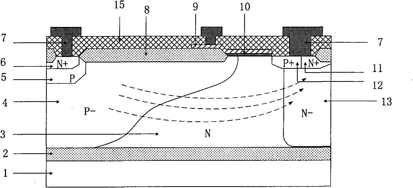
[0024] Attached below figure 1 , the present invention is described in detail, a P-type lateral insulated gate bipolar device that reduces the hot carrier effect, comprising: an N-type substrate 1, a buried oxygen 2 is arranged on the N-type substrate 1, and a buried oxygen 2 is provided with an N-type epitaxial layer 3, a P-type well 4 and an N-well region 13 are provided on the N-type epitaxial layer 3, a P-type buffer well 5 is provided on the P-type well 4, and a P-type buffer well 5 is provided on the P-type buffer well 5. An N-type positive region 6 is provided, a P-type negative region 12 and an N-type body contact region 11 are arranged on the N well region 13, and a gate oxide layer 10 is arranged on the surface of the N-type epitaxial region 3, and the gate oxide layer 10 is formed from N The epitaxial region 3 extends to the P-type well region 4, and a field oxide layer 8 is provided in the area other than the N-type anode region 6, the N-type body contact region 1...


PUM


Abstract

The invention relates to a P type lateral insulated gate bipolar device for reducing the hot carrier effect, comprising an N type substrate. Buried oxide is arranged on the N type substrate, an N type epitaxial layer is arranged on the buried oxide, a P type well and an N well region are arranged on the N type epitaxial layer, a P type buffer well is arranged on the P type well, an N type positive region is arranged on the P type buffer well, a P type negative region and an N type physical contact region are arranged on the N well region, and a field oxide, a metal layer, a gate oxide, a polysilicon gate and an oxide layer arranged on the surface of the device. The P type lateral insulated gate bipolar device for reducing the hot carrier effect is characterized in that N type buried layers are arranged at the lower part of the N well region and on the buried oxide, and the N type buried layers are partially inserted into the N type epitaxial layer to integrally form a reverse L type N region with the N well region. The structure can introduce the electronic current of the device to the bottom, reduce ion generation rate and longitudinal field of a channel region of the device, and lower the thermionic temperature, thereby effectively restraining the hot carrier effect of the device.

Description

technical field [0001] The invention relates to the field of high-voltage power semiconductor devices, and relates to a P-type lateral insulating gate bipolar device suitable for high-voltage applications and reducing hot carrier effects. Background technique [0002] Power semiconductor devices are the basic electronic components for energy control and conversion in power electronic systems. The continuous development of power electronics technology has opened up a wide range of application fields for semiconductor power devices, and the characteristics of semiconductor power devices such as on-resistance and breakdown voltage determine The basic performance of the power electronic system, such as efficiency and power consumption. [0003] With the increasing demand for modern life, the performance of power integrated circuits has attracted more and more attention, and the life of power integrated circuits has increasingly become one of the most important performance indica...

Claims


Application Information

Patent Timeline
IPC IPC(8): H01L29/735H01L29/06
Inventor 钱钦松刘斯扬孙伟锋毛宁陆生礼时龙兴
Owner SOUTHEAST UNIV
Learn More