Magnetoelectric random storage unit and storage with same

A random access storage and memory technology, applied in the field of semiconductor manufacturing and design, can solve the problems of excessive power consumption of magnetic random access memory and the influence of adjacent cells, and achieve the effects of reducing write power consumption, improving storage density, and reducing interference

Active Publication Date: 2011-09-14
TSINGHUA UNIV
View PDF0 Cites 0 Cited by
  • Summary
  • Abstract
  • Description
  • Claims
  • Application Information

AI Technical Summary

Problems solved by technology

[0005] The present invention aims to solve at least one of the above-mentioned technical problems in the prior art, especially to solve the problem of excessive power consumption and impact on adjacent cells caused by the existing magnetic random access memory using a current to generate a magnetic field for writing operations

Method used


Image

  • Magnetoelectric random storage unit and storage with same
  • Magnetoelectric random storage unit and storage with same
  • Magnetoelectric random storage unit and storage with same

Examples


no. 1 example

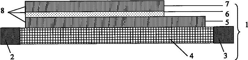
[0063] Prepare the ferroelectric oxide layer 4 as lead niobate zincate-lead titanate (PZN-PT) with a thickness of 250nm, and deposit 5nm thick Fe with (001) orientation 0.7 co 0.3 The ferromagnetic free layer 5 of the alloy, the magnesium oxide (MgO) tunnel barrier layer 6 with a thickness of 1.5nm, and the ferromagnetic fixed layer 7 of the CoFeB alloy with a thickness of 25nm, the ferromagnetic free layer 5 and the tunnel barrier layer obtained by etching technology 6. The multilayer composite film structure of the ferromagnetic fixed layer 7 has a length of 1 μm and a width of 0.5 μm. Apply a voltage parallel to the film length direction in the ferroelectric oxide layer 4, Figure 6 In this system, the resistance value of the interlayer structure 8 varies with the voltage applied to the ferroelectric oxide layer 4. In this system, the positive critical switching voltage U cr is 0.72V, the negative critical switching voltage U cr is 0.51V.

[0064] As shown in the above ...

no. 2 example

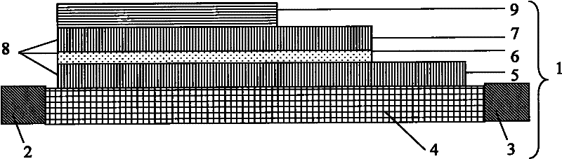
[0066] Prepare the ferroelectric oxide layer 4 as barium titanate (BTO) with a thickness of 250nm, deposit 5nm thick Fe with (001) orientation 0.7 co0.3 The ferromagnetic free layer 5 of the alloy, the magnesium oxide (MgO) tunnel barrier layer 6 with a thickness of 1.5nm, and the ferromagnetic fixed layer 7 of the CoFeB alloy with a thickness of 25nm, the ferromagnetic free layer 5 and the tunnel barrier layer obtained by etching technology 6. The ferromagnetic fixed layer 7 has a multilayer composite film structure with a length of 1 μm and a width of 0.5 μm. Apply a voltage parallel to the film length direction in the ferroelectric oxide layer 4, Figure 7 In this system, the resistance of the composite structure varies with the voltage applied to the ferroelectric oxide layer. In this system, the positive critical switching voltage U cr is 9.7V, the negative critical switching voltage U cr is 6.8V. As shown in the figure, due to the same principle as that of Embodiment ...

no. 3 example

[0068] Prepare a ferroelectric oxide layer of lead zirconate titanate (PZT) with a thickness of 250nm, deposit 5nm thick Fe with (001) orientation 0.7 co 0.3 Alloy ferromagnetic free layer, 1.5nm thick magnesium oxide (MgO) tunnel barrier layer, and 25nm thick CoFeB alloy ferromagnetic pinned layer, ferromagnetic free layer, tunnel barrier layer, ferromagnetic pinned layer obtained by etching technology The layer composite structure has a length of 1 μm and a width of 0.5 μm. Applying a voltage parallel to the lengthwise direction in the ferroelectric oxide layer, Figure 8 In this system, the resistance of the composite structure varies with the voltage applied to the ferroelectric oxide layer. In this system, the positive critical switching voltage U cr is 4.5V, the negative critical switching voltage U cr is 3.2V. As shown in the figure, due to the same principle as that of Embodiment 1, it shows that the random storage unit has non-volatile storage.

[0069] The embod...


PUM


Abstract

The invention discloses a memorizer having a magnetoelectric random storage unit, comprising a plurality of magnetoelectric random storage units; a plurality of access transistors connected to first electrodes in the magnetoelectric random storage units; a plurality of word lines for controlling the access transistors; a plurality of first printed lines connected to second electrodes in the magnetoelectric random storage units; a plurality of first bit lines connected to the access transistors; a plurality of second bit lines connected to ferroelectric fixed layers in the magnetoelectric random storage units; and a plurality of second printed lines connected to ferromagnetic free layers in the magnetoelectric random storage units. The embodiment of the invention can write in information data with the electric field, and has the advantages of nonvolatility, low write-in power consumption, high storage density and the like.

Description

technical field [0001] The invention relates to the technical field of semiconductor manufacturing and design, in particular to a magnetoelectric random access memory unit and a random access memory with the magnetoelectric random access memory unit. Background technique [0002] Magnetic Random Access Memory (MRAM) is a non-volatile memory that utilizes the magnetoresistance effect for data storage. The magnetoresistance effect is the effect that the electrical resistance of a material changes under the action of a magnetic field. The three-layer structure composed of ferromagnetic layer, tunnel barrier layer and ferromagnetic layer is a typical structure with magnetoresistance effect. When the magnetization directions of the ferromagnetic layers above and below the tunnel barrier layer are consistent, the resistance of the structure is minimum. Under the action of a magnetic field, the magnetization direction in the ferromagnetic layer tends to be oriented towards the di...

Claims


Application Information

Patent Timeline
Patent Type & Authority Patents(China)
IPC IPC(8): H01L43/00H01L27/22
Inventor 南策文李峥舒立胡嘉冕王婧马静林元华
Owner TSINGHUA UNIV
Why Eureka
Try Eureka