Orthogonal input and orthogonal output frequency-halving device with low power consumption and low stray

A two-frequency divider and output terminal technology is applied in the design field of quadrature input and quadrature output frequency dividers, which can solve the problems of large operating frequency range, low power consumption, and the inability of frequency dividers to handle quadrature signals.

CN101834603AInactive Publication Date: 2010-09-15FUDAN UNIV
0 Cites 6 Cited by

Patent Information

Authority / Receiving Office
CN · China
Current Assignee / Owner
Publication Date
2010-09-15
Estimated Expiration
Not applicable · inactive patent

Smart Images

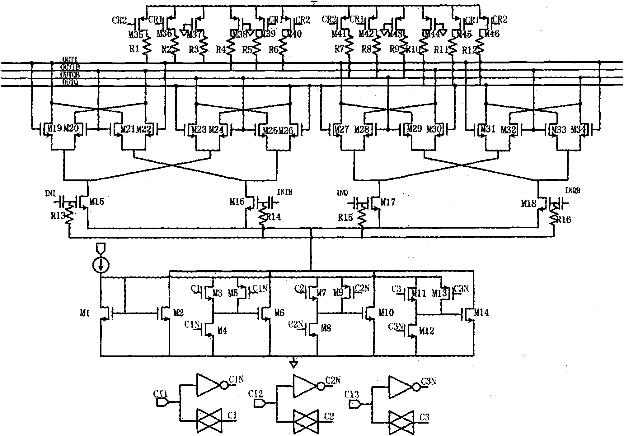
  • Figure 1
    Figure 1
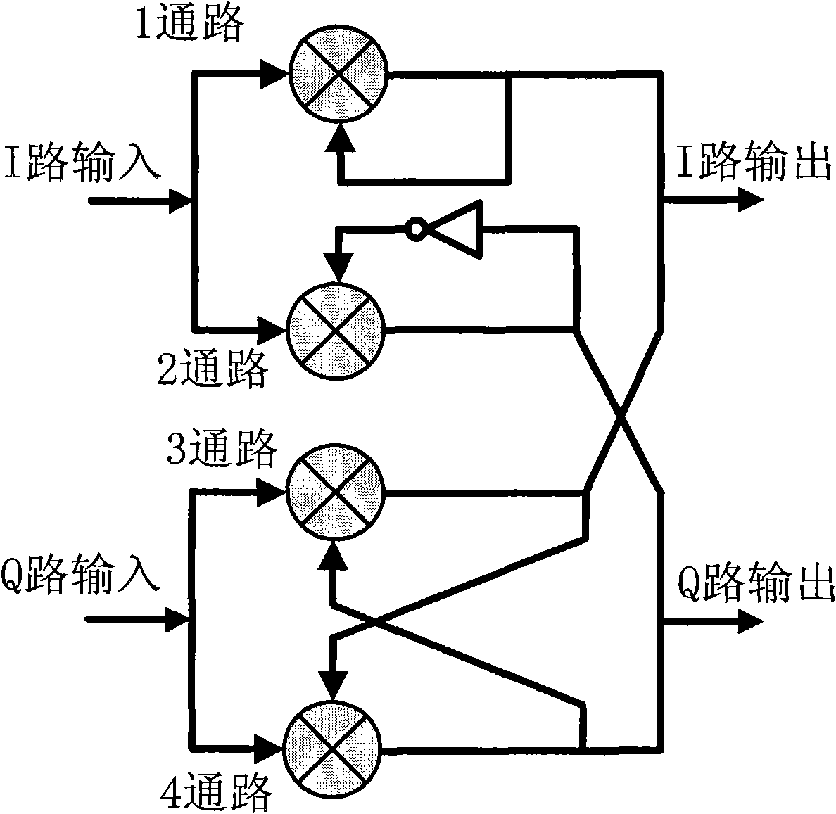
  • Figure 2
    Figure 2
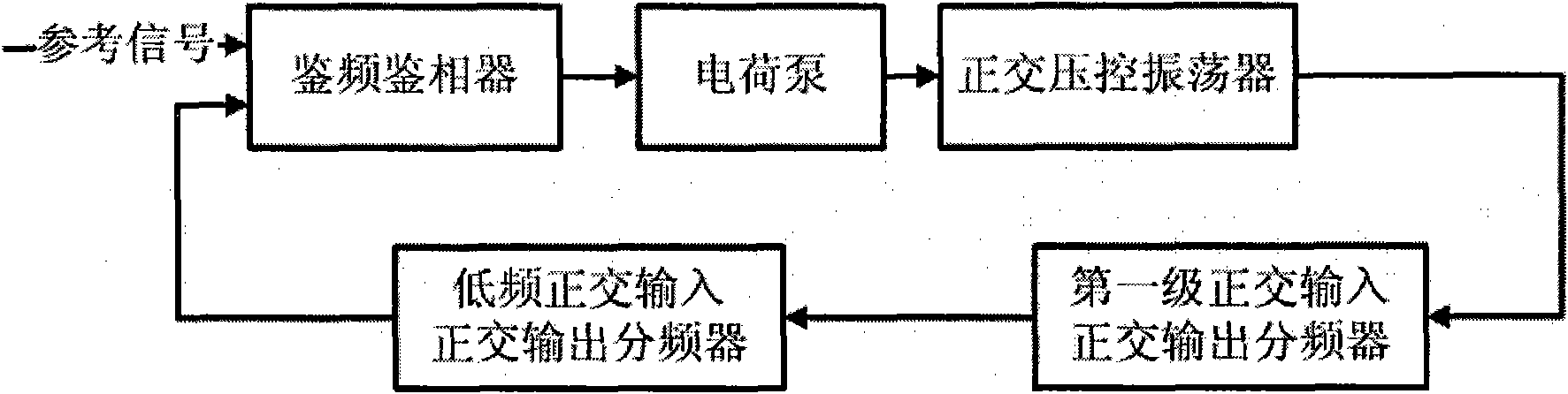
  • Figure 3
    Figure 3
Patent Text Reader

Abstract

The invention relates to an orthogonal input and orthogonal output frequency-halving device with low power consumption and low stray, belonging to the technical field of integrated circuits of radio-frequency wireless receivers. The frequency-halving device comprises variable load stage, input transconductance stage, mixing stage and variable current source bias circuits. Compared with traditional source coupled logic frequency-halving circuit and Miller frequency-halving circuit, the invention can realize higher working frequency and higher triple-harmonic inhibition under the condition of lower power consumption, and the process deviation and the temperature deviation are insensitive.
Need to check novelty before this filing date? Find Prior Art

Description

technical field

[0001] The invention belongs to the technical field of radio frequency wireless receiver integrated circuits, and in particular relates to the design of a quadrature input quadrature output frequency divider (Quadrature Input Quadrature Output Frequency Divider) applied in a wireless receiver integrated circuit, which can realize high frequency The signal is divided by two. Background technique

[0002] With the development of modern information technology, the requirements for high data rate and large bandwidth of wireless communication technology are becoming more and more intense, which prompts people to continuously develop higher frequency band resources and study ultra-high frequency wireless communication technology. At the same time, under the inevitable trend of the development of modern integrated circuits to the direction of system chips, low power consumption design has become an inevitable requirement for circuit design of various communication s...

Examples

Embodiment Construction

[0011] Applying the quadrature input quadrature output frequency divider of the present invention to the frequency of the dual-carrier Orthogonal Frequency Division Multiplexing Ultra-Wide Band (Double Carrier Orthogonal Frequency Division Multiplexing Ultra-Wide Band) radio frequency receiver in the 6.0GHz to 9.0GHz frequency band In the synthesizer system, image 3 Shown is a schematic diagram of the structure of the phase-locked loop in the frequency synthesizer, which consists of a frequency and phase detector, a charge pump, a loop filter, a voltage-controlled oscillator and a frequency divider chain. The frequency and phase detector detects the frequency difference and phase difference between the crystal oscillator (reference clock) and the output signal of the frequency divider, and converts the difference into a current signal through the charge pump, and the current flows into the loop filter A voltage signal is formed to adjust the frequency of the voltage-controlle...