CCD (Charge Coupled Device) galvanometer type laser welding device and method

A technology of laser welding and welding position, which is applied in the direction of laser welding equipment, auxiliary equipment, welding equipment, etc., to achieve the effect of simple equipment and reducing pollution

Active Publication Date: 2010-09-15
UNITED AUTOMOTIVE ELECTRONICS SYST
View PDF0 Cites 15 Cited by
  • Summary
  • Abstract
  • Description
  • Claims
  • Application Information

AI Technical Summary

Problems solved by technology

[0006] The technical problem to be solved by the present invention is to dynamically and accurately control the welding position without causing pollution

Method used


Image

  • CCD (Charge Coupled Device) galvanometer type laser welding device and method
  • CCD (Charge Coupled Device) galvanometer type laser welding device and method

Examples


Embodiment Construction

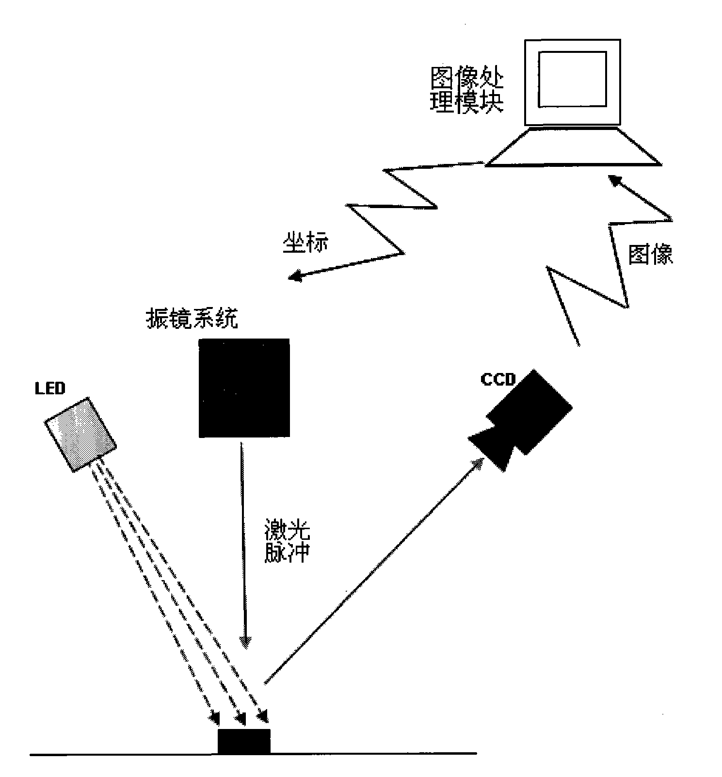
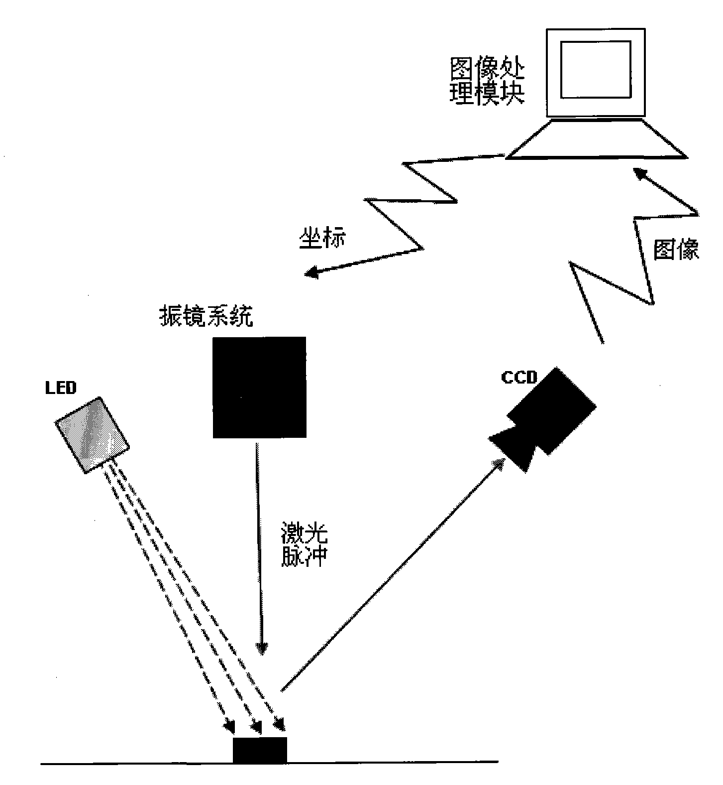
[0018] One embodiment of the CCD galvanometer type laser welding device and method of the present invention is as follows figure 1 As shown, it includes LED lights, CCD (Charge Coupled Device, Charge Coupled Device) image acquisition device, image processing module, galvanometer system (there are two mirrors driven by high-precision servo motors inside the galvanometer system, and the servo motor is controlled by a microcomputer. The angles of the two reflectors are respectively rotated under the control of the two reflectors, and the laser is focused on different positions of the workpiece through the reflection of the two reflectors), the electronic components to be welded are placed on the printed circuit board (PCB) and the pins of the electronic components The position that needs to be soldered is in close contact with the corresponding soldering point on the pad of the printed circuit board, and the LED light is used to obliquely illuminate the pin of the electronic compo...


PUM


Abstract

The invention discloses a CCD (Charge Coupled Device) galvanometer type laser welding device which comprises an LED lamp, a CCD image acquisition device, an image processing module and a galvanometer system, wherein the LED lamp is used for obliquely irradiating an electronic component pin from the side face of the electronic component pin to project the shadow of the electronic component pin onto a printed circuit board; the CCD image acquisition device is used for acquiring the image data of the electronic component pin through the light and shade contrast on the printed circuit board; the image processing module is used for calculating according to the image data to obtain a welding position coordinate of the electronic component pin and conveying the welding position coordinates to the galvanometer system; and the galvanometer system is used for emitting laser pulses according to the information of the welding position coordinate to smelt the electronic component pin material and form a welding spot on the printed circuit board. The invention also discloses a CCD galvanometer type laser welding method. The invention can dynamically and precisely control the welding position and is not easy to cause pollution.

Description

technical field [0001] The invention relates to electronic device welding technology, in particular to a CCD vibrating mirror type laser welding device and method. Background technique [0002] In view of the characteristics of many pins (Pin) and small spacing in electronic components, the current methods of soldering electronic devices are wave soldering, reflow soldering, selective soldering, soldering with semiconductor laser, etc. Although these methods are suitable for mass production , but there are also some problems: [0003] 1. The process and equipment are complex. For example, in wave soldering, the amount of flux sprayed, preheating temperature, preheating time, soldering temperature, soldering time, conveyor belt inclination angle, peak height, etc. are all factors that affect the quality, and various soldering parameters affect each other. To obtain A good welding effect requires a comprehensive adjustment of the process parameters. [0004] 2. High require...

Claims


Application Information

Patent Timeline
Patent Type & Authority Applications(China)
IPC IPC(8): H05K3/34B23K26/20B23K1/005B23K3/00B23K3/08
Inventor 朱晓伟王东阳王学全丁慧明
Owner UNITED AUTOMOTIVE ELECTRONICS SYST
Why Eureka
Try Eureka