Indium-arsenic quantum dot active region structure and light emitting device
An indium arsenic quantum, light-emitting device technology, applied in phonon exciters, laser components, lasers, etc., can solve the problems of reduced luminous intensity, weakened quantum confinement effect, reduced barrier height of InAs quantum dots, etc., to achieve large luminescence Effects of Efficiency and Luminous Intensity
- Summary
- Abstract
- Description
- Claims
- Application Information
AI Technical Summary
Problems solved by technology
Method used
Image

Examples
Embodiment 1
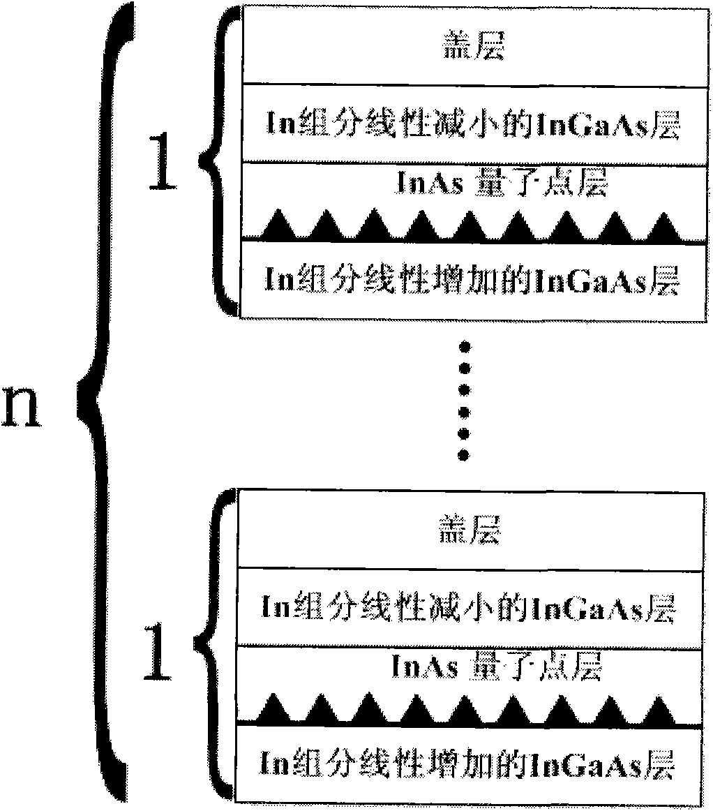
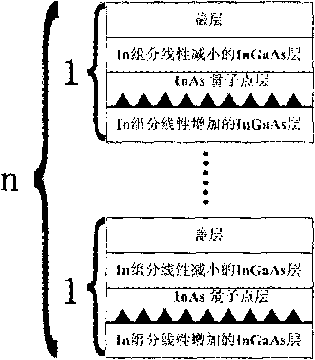
[0029] Embodiment 1.InAs quantum dot active region structure
[0030] The InAs quantum dot active region structure, such as figure 1Shown: it contains n InAs quantum dot layers 1, n≥1. For simplicity, in figure 1 Only two InAs quantum dot layers are drawn in the figure, and the others are represented by ".". In the actual InAs quantum dot active region structure, it is often not just one quantum dot layer, but to use multiple quantum dot layers to obtain large gain and luminous intensity. At this time, the quantum dot active region structure will contain multiple individual such as figure 1 InAs quantum dot layer 1 is shown.
[0031] For each InAs quantum dot layer 1, such as figure 1 As shown: it epitaxially grows an InGaAs layer with a linearly increasing In composition, an InAs quantum dot layer, an InGaAs layer with a linearly decreasing In composition, and a capping layer sequentially from bottom to top.
[0032] The capping layer may be composed of a single layer m...
Embodiment 2
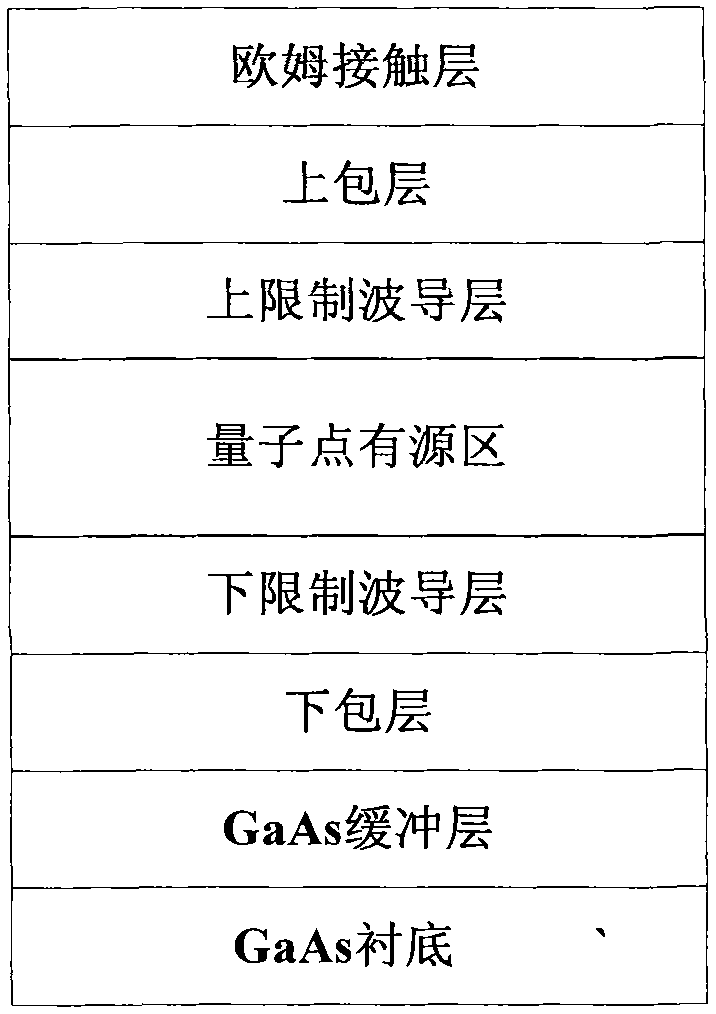
[0041] Embodiment 2.InAs quantum dot light-emitting device
[0042] figure 2 It is a structural schematic diagram of the InAs quantum dot light-emitting device of the present invention, which can be applied to quantum dot lasers, superluminescent light-emitting tubes, light-emitting diodes and semiconductor optical amplifiers. figure 2 The quantum dot light-emitting device in the method is epitaxially growing GaAs buffer layer, lower cladding layer, lower confinement waveguide layer, quantum dot active region, upper confinement waveguide layer, upper cladding layer, and ohmic contact layer on the GaAs substrate sequentially from bottom to top.
PUM
| Property | Measurement | Unit |
|---|---|---|
| thickness | aaaaa | aaaaa |
| thickness | aaaaa | aaaaa |
| thickness | aaaaa | aaaaa |
Abstract
Description
Claims
Application Information
 - Generate Ideas
- Intellectual Property
- Life Sciences
- Materials
- Tech Scout
- Unparalleled Data Quality
- Higher Quality Content
- 60% Fewer Hallucinations
Browse by: Latest US Patents, China's latest patents, Technical Efficacy Thesaurus, Application Domain, Technology Topic, Popular Technical Reports.
© 2025 PatSnap. All rights reserved.Legal|Privacy policy|Modern Slavery Act Transparency Statement|Sitemap|About US| Contact US: help@patsnap.com