

Method for making optical waveguides
A technology of wave guide and ring resonator, applied in the field of preparing optical wave guide, can solve the problem of high tensile stress value, and achieve the effects of reducing annealing temperature, reducing stress and improving equipment quality
- Summary
- Abstract
- Description
- Claims
- Application Information
AI Technical Summary
Problems solved by technology
Method used
Image

Examples
example 1
[0034] Example 1: With SiO 2 / SiN Ridge / SiO 2 Interlayer (annealed) ring resonator
[0035] The invention is demonstrated by the fabrication of vertically connected ring resonators with a diameter of 100 μm. The ring resonator was fabricated as follows.
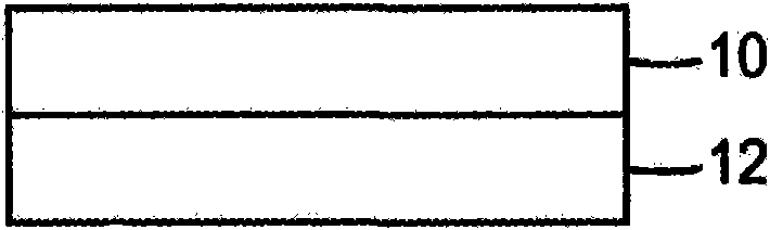
[0036] By plasma enhanced chemical vapor deposition (PEVCD, available from Oxford Instruments, Yatton, UK, model P1asmaLab using the following parameters listed in Table 1 TM system 100), a 3 μm thick lower cladding layer of borophosphosilicate glass (BPSG) with a refractive index of 1.46 was deposited on a 0.5 mm Si wafer (100) (Si wafers can be purchased from Montco Silicon Technologies of Spring City, PA. company) on.
[0037] Table 1. Conditions used to deposit BPSG lower cladding
[0038] Reactants / Conditions:
value:
SiH 4
17 sccm
B 2 h 6
3.5 sccm
pH 3
1.8 sccm
N 2 o
1500 sccm
N 2
600 sccm
RF power
130W
pre...
example 2 and example 3
[0062] Example 2 and Example 3: Fabrication of ridge SiON core layer (patterning; annealing)
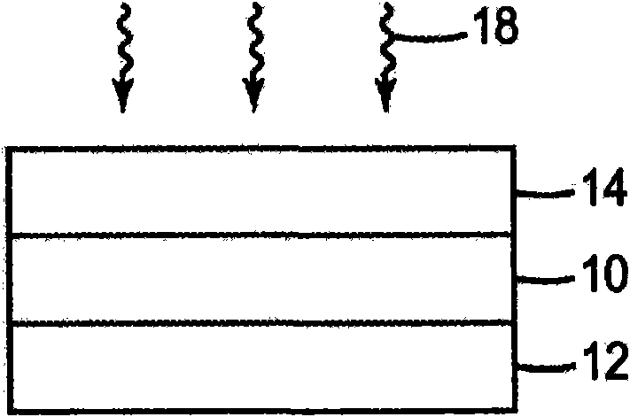
[0063] Several Si wafers prepared as described in Comparative Example 2 coated with a 700 nm thick SiON coating were coated with PR and the PR layer was patterned using a waveguide pattern mask and standard photolithographic techniques. Reactive ion etching was performed according to the conditions described in Table 3 to form ridged waveguide cores (100 μm ridges in Example 2; 50 μm ridges in Example 3).
[0064] The SiON core layers of Example 2 and Example 3 were annealed for 30 minutes at temperatures of 600°C, 700°C, 800°C, 900°C and 1000°C in a furnace with a heating and cooling rate of 2°C / min. The SiON core is crack-free when viewed using optical microscopy.
example 4
[0073] Example 4: With SiO 2 / a-Si ridge / SiO 2 Interlayer (annealed) ring resonator
[0074] By plasma enhanced chemical vapor deposition (PEVCD, available from Oxford Instruments in Yatton, UK, model PlasmaLab using the parameters listed in Table 1 TM System 100) of 3 μm thick borophosphosilicate glass (BPSG) lower cladding with a refractive index of 1.46 was deposited on a 0.5 mm Si wafer (100) (Si wafers can be purchased from Montco Silicon Technologies in SpringCity, PA) superior.
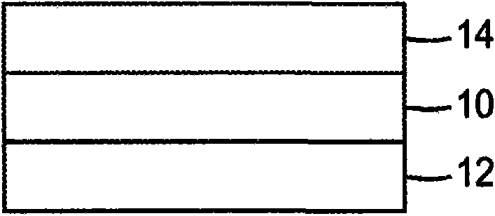
[0075] After the BPSG layer was formed on the Si wafer, the sample was heated to 1080° C. in a furnace at a ramp rate of 5° C. / min and kept at that temperature for about 4 hours to allow the BPSG to reflow. After heat treatment, a 250 nm thick amorphous silicon (a-Si) core layer was deposited on the BPSG lower cladding layer by PECVD using the following parameters described in Table 7.
[0076] Table 7. Conditions used to deposit a-Si layer
[0077] Reactants / Condition...
PUM
| Property | Measurement | Unit |
|---|---|---|
| thickness | aaaaa | aaaaa |
| etching depth | aaaaa | aaaaa |
| refractive index | aaaaa | aaaaa |
Abstract
Description
Claims
Application Information