Manufacturing method and device of winding banded ITO conductive film

A technology of conductive film and production method, applied in ion implantation plating, metal material coating process, coating and other directions, can solve the problem that sheet-type products cannot meet the requirements of large-scale products, many production processes, and poor product performance consistency and other problems, to achieve the effect of good product performance consistency, improved quality, and large width.

Active Publication Date: 2010-12-15
HUAIAN FUYANG ELECTRONICS MATERIALS
View PDF3 Cites 11 Cited by
  • Summary
  • Abstract
  • Description
  • Claims
  • Application Information

AI Technical Summary

Problems solved by technology

[0003] The conductive films currently produced in the market are limited to chip production, and chip products cannot meet the requirements of large-scale products, and there are many production processes, resulting in poor consistency of product performance.

Method used


Image

  • Manufacturing method and device of winding banded ITO conductive film
  • Manufacturing method and device of winding banded ITO conductive film

Examples


Embodiment 1

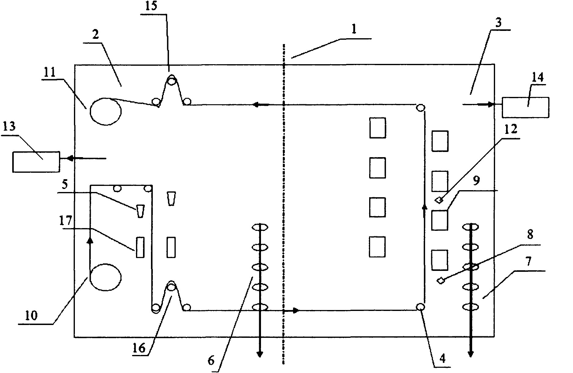
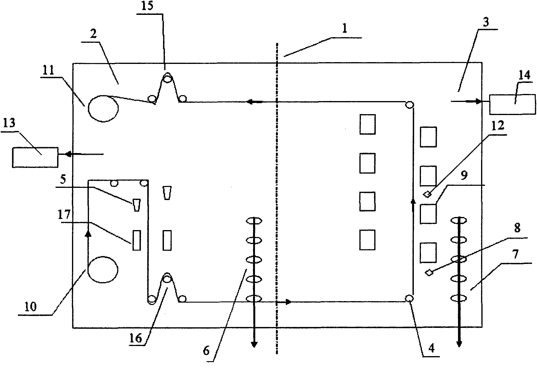
[0015] The ITO conductive film is produced according to the following steps: first, the substrate is in the discharge chamber, and the surface of the substrate is treated by an infrared heater and an ion source in a vacuum state; secondly, it enters the sputtering chamber, and the substrate is sprayed Sputter silicon dioxide film on top; then, sputter indium tin oxide film on the silicon dioxide film; finally, leave the studio for cutting and packaging; among them, the power of linear ion source is 2kw; the power of infrared heater is 300W, the temperature 100°C; the vacuum degree of the sputtering chamber is 1×10 -3 pa, the sputtering atmosphere is formed by oxygen and argon with a mass ratio of 0.2:5; silicon dioxide film: the sputtering power is 200w, the sputtering target is quartz with a purity greater than 99.99%, and the sputtering power supply is radio frequency sputtering power supply; Indium tin oxide film: the sputtering power is 500w, the sputtering target is a cer...

Embodiment 2

[0017] The ITO conductive film is produced according to the following steps: first, the substrate is in the discharge chamber, and the surface of the substrate is treated by an infrared heater and an ion source in a vacuum state; secondly, it enters the sputtering chamber, and the substrate is sprayed sputtering silicon dioxide film on top; then, sputtering indium tin oxide film on the silicon dioxide film; finally, leaving the working room for cutting and packaging; among them, the power of the linear ion source is 6kw; the power of the infrared heater is 550W, and the temperature 115°C; the vacuum degree of the sputtering chamber is 3×10 -3 pa, the sputtering atmosphere is formed by oxygen and argon with a mass ratio of 0.2:5.5; silicon dioxide film: the sputtering power is 350w, the sputtering target is quartz with a purity greater than 99.99%, and the sputtering power supply is radio frequency sputtering power supply; Indium tin oxide film: the sputtering power is 650w, th...

Embodiment 3

[0019] The ITO conductive film is produced according to the following steps: first, the substrate is in the discharge chamber, and the surface of the substrate is treated by an infrared heater and an ion source in a vacuum state; secondly, it enters the sputtering chamber, and the substrate is sprayed Sputter silicon dioxide film on top; then, sputter indium tin oxide film on the silicon dioxide film; finally, leave the studio for cutting and packaging; among them, the power of linear ion source is 10kw; the power of infrared heater is 800W, the temperature 130°C; the vacuum degree of the sputtering chamber is 5×10 -3 pa, the sputtering atmosphere is formed by oxygen and argon with a mass ratio of 0.2:6; silicon dioxide film: the sputtering power is 500w, the sputtering target is quartz with a purity greater than 99.99%, and the sputtering power supply is radio frequency sputtering power supply; Indium tin oxide film: the sputtering power is 800w, the sputtering target is a ce...


PUM


Abstract

The invention discloses a manufacturing method of a winding banded ITO conductive film, a substrate is placed in a material preparation chamber and the surface is processed through an infrared heater and an ion source in a vacuum condition; the substrate enters a sputtering chamber, and a sputtering target and a silica dispenser are used for sputtering a silica film on the substrate; an indium tin oxide film is sputtered on the silica film; a transmission rack (4) is arranged in the material preparation chamber (2) and the sputtering chamber (3), the front and tail ends of the transmission rack (4) are both arranged in the material preparation chamber (2), a discharging roller (10) and a receiving roller (11) are respectively arranged at the front and tail ends of the transmission rack (4), the infrared heater (17) and the ion source (5) are respectively arranged at two sides of the transmission rack (4) in the material preparation chamber (2), the sputtering target (9) is arranged at two sides of the transmission rack (4) in the sputtering chamber (3), and the silica dispenser (8) and an indium tin oxide dispenser (12) are respectively arranged in the front and middle of the sputtering target (9) in the sputtering chamber (3). The method and the device sputter coatings on the substrate and can realize continuous production, increase the product width and length and enlarge the product use.

Description

technical field [0001] The invention belongs to the technical field of electronic materials, and relates to a production method and a device of a conductive film, in particular to a production method and a device of a winding strip-shaped ITO conductive film. Background technique [0002] As we all know, the development trend of electronic products is to develop in the direction of thin and light, small space occupation, and easy to carry. The market demand for transparent conductive films in the fields of flat panel displays, solar cells, large-area transparent electromagnetic shielding, and large-area touch screens is increasing. . [0003] The conductive films currently produced in the market are limited to chip production, and chip products cannot meet the requirements of large-scale products, and there are many production processes and poor consistency of product performance. Contents of the invention [0004] The object of the present invention is to: provide a kind...

Claims


Application Information

Patent Timeline
Patent Type & Authority Applications(China)
IPC IPC(8): C23C14/34C23C14/02C23C14/10C23C14/08C23C14/56
Inventor 傅青炫陈先锋马尔松夏慎领
Owner HUAIAN FUYANG ELECTRONICS MATERIALS
Why Eureka
Try Eureka