Method for manufacturing printed circuit board by power triggering electroless plating addition process

A printed circuit board and electroless plating technology, applied in printed circuit, printed circuit manufacturing, liquid chemical plating, etc., can solve the problems of expensive inkjet printing equipment, limited thickness of chemical plating layer, poor bonding force of plating layer, etc., and achieve easy operation , less control process parameters, fast plating effect

Active Publication Date: 2010-12-22
GUANGDONG UNIV OF TECH +1
View PDF2 Cites 6 Cited by
  • Summary
  • Abstract
  • Description
  • Claims
  • Application Information

AI Technical Summary

Problems solved by technology

The first method still involves an etching process, not an additive method in the true sense; the second method has problems such as expensive inkjet printing equipment, easy catalyst failure, limited thickness of the electroless plating layer, and poor bonding force of the plating layer.

Method used


Image

  • Method for manufacturing printed circuit board by power triggering electroless plating addition process
  • Method for manufacturing printed circuit board by power triggering electroless plating addition process

Examples


Embodiment 1

[0027] The present invention takes polyester film as an example to print carbon paste patterns on the screen and electroless copper plating on the carbon paste patterns to illustrate the manufacturing process of PCB circuit patterns in detail.

[0028] Table 1 Formula of electroless copper plating solution

[0029]

[0030] Chemical reagent Concentration g / L

[0031]

[0032] CuSO 4 ·5H 2 O 16

[0033] Sodium Potassium Tartrate 14

[0034] Disodium edetate 19.5

[0035] Sodium hydroxide 14.5

[0036] Potassium iodide 0.015

[0037] HCHO (formaldehyde) 15ml / L

[0038] pH 12~12.5

[0039] Temperature ℃ 40~50

[0040]

[0041] The specific experimental steps are as follows:

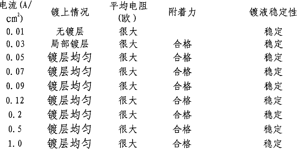
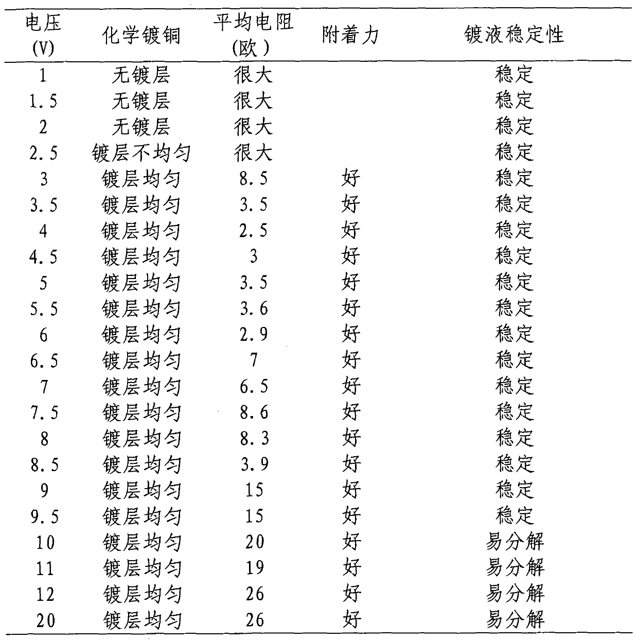
[0042] (1) make a 15cm * 15cm * 10cm with plexiglass, the cuboid without top is used as the chemical plating tank body;

[0043] (2) Graphite is used...

Embodiment 2

[0053] The present invention takes the electroless nickel plating of polyester film with carbon paste pattern printed on the screen as an example, and specifically illustrates the PCB circuit pattern manufacturing process.

[0054] Table 3 Formula of electroless nickel plating solution

[0055]

[0056] Chemical reagent Concentration g / L

[0057]

[0058] NiSO 4 ·6H 2 O 25

[0059] Citric acid 6

[0060] Sodium succinate 5

[0061] Ammonium acetate 4.5

[0062] Glycine 1

[0063] Lactic acid 8ml / L

[0064] NaH 2 PO 2 ·H 2 O 25

[0065] pH 4.8~5.2

[0066] Temperature ℃ 80~85

[0067]

[0068] The specific experimental steps are as follows:

[0069] 1. Use plexiglass to make a 15cmX15cmX10cm, cuboid without a roof as the chemical plating tank;

[0070] 2. Use graphite as the anode material, connect to the positive pole o...


PUM


Abstract

The invention discloses a method for manufacturing a printed circuit board by a power triggering electroless plating addition process. The method comprises the following the steps: forming circuit patterns made of conducting materials on a non-conducting substrate in various printing modes; soaking the prepared circuit patterns in an electroless plating solution; placing two electrodes in the electroless plating solution, connecting the inertia positive electrode with the positive electrode of a DC constant-voltage or constant-current power source, and connecting the negative electrode with the negative electrode of the DC constant-voltage or constant-current power source; powering on after setting the voltage or current, utilizing the circuit patterns printed by contact of the negative electrode to trigger the electroless plating process, and depositing metal on the circuit patterns; and after carrying out electroless plating for 30 minutes, taking out the circuit patterns and cleaning, thus obtaining the metalized circuit patterns. The method of the invention has no need of carrying out activating treatment on the printed circuit patterns, less operating steps, less control process parameters, easy operation, high plating speed and even plating.

Description

technical field [0001] The invention belongs to the technical field of surface chemical treatment of materials, and in particular relates to a method for manufacturing printed circuit boards (PCBs) by an additive method of electric-induced electroless plating. Background technique [0002] Printed circuit boards (PCBs) are widely used in computer motherboards, graphics cards, network cards, memory sticks, power supplies, hard drives, optical drives and other components. Not only that, but various electrical appliances such as refrigerators, washing machines, air conditioners, home theaters, DVDs, and mobile phones used in daily life are inseparable from printed circuit boards. Even in industry, agriculture, scientific research, aerospace, aviation and other places where automation and electrification are required, printed circuit boards are indispensable. In other words, printed circuit boards are ubiquitous in modern society. [0003] Modern printed circuit manufacturing ...

Claims


Application Information

Patent Timeline
Patent Type & Authority Applications(China)
IPC IPC(8): C23C18/31H05K3/18
Inventor 胡光辉罗观和陈世荣潘湛昌张惠冲魏志钢
Owner GUANGDONG UNIV OF TECH
Why Eureka
Try Eureka