Silicon carbide semiconductor device

A technology of semiconductor and silicon carbide, which is applied in the field of silicon carbide semiconductor devices, can solve the problems such as the reduction of withstand voltage characteristics of silicon carbide semiconductor devices, and achieve the effect of realizing the stability of withstand voltage

Inactive Publication Date: 2011-01-12
MITSUBISHI ELECTRIC CORP
View PDF3 Cites 6 Cited by
  • Summary
  • Abstract
  • Description
  • Claims
  • Application Information

AI Technical Summary

Problems solved by technology

In this way, if the electric field is concentrated on the terminal portion, the withstand voltage characteristics of the silicon carbide semiconductor device will be reduced.

Method used


Image

  • Silicon carbide semiconductor device
  • Silicon carbide semiconductor device
  • Silicon carbide semiconductor device

Examples


Embodiment approach 1

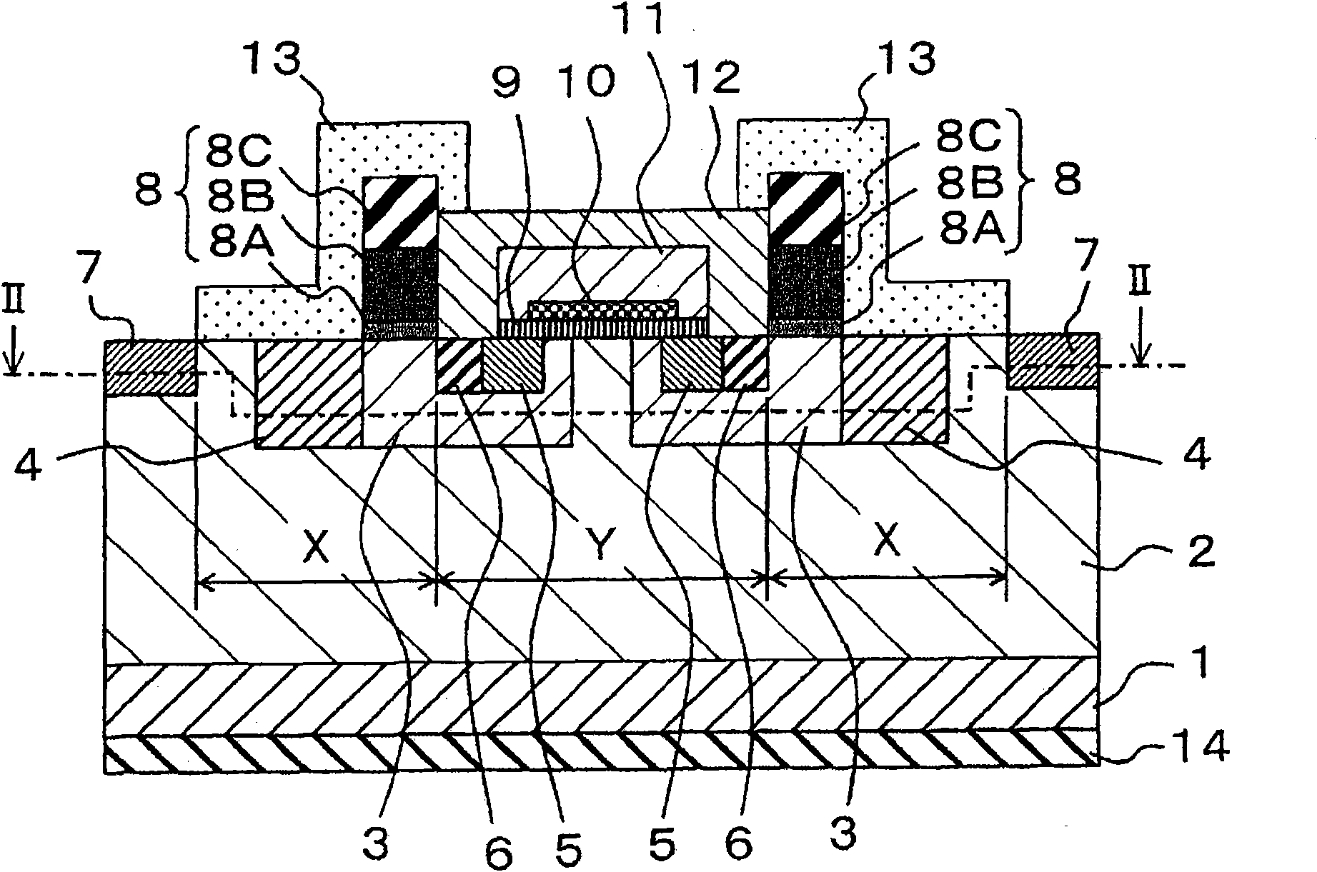
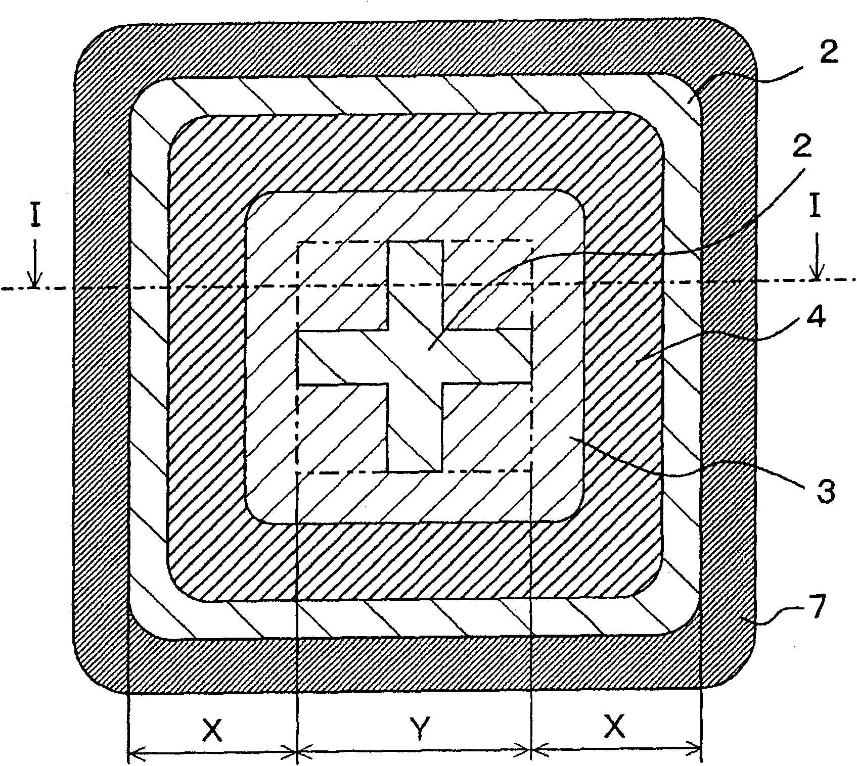
[0061] figure 1 A cross-sectional structure of the silicon carbide semiconductor device according to Embodiment 1 of the present invention viewed from a side direction is shown. in addition, figure 2 A cross-sectional structure viewed from the upper direction is shown. Here, as a silicon carbide semiconductor device, a cross-sectional structure of a power MOSFET (Power Metal Oxide Semiconductor Field Effect Transistor) is shown. in addition, figure 1 Shows figure 2 The I-I profile in, figure 2 Shows figure 1 The II-II profile in . in addition, Figure 3 to Figure 12 Shows figure 1 as well as figure 2 The fabrication method of the power MOSFET is shown.

[0062] First, refer to figure 1 as well as figure 2 , to explain the structure of the power MOSFET.

[0063] 1 is n + type (first conductivity type) semiconductor substrate. 2 is n - Type (first conductivity type) silicon carbide layer (drift layer). 3 is a p-type (second conductivity type) well region as...

Embodiment

[0090] In this example, first make Figure 14 to Figure 17 The test samples (test sample A to test sample D) having four kinds of MOS capacitors as shown, and the flat band voltage was measured for each test sample. Then, the effective fixed charge density of each test sample was evaluated based on the shift amount of the flat band voltage.

[0091] Test samples A and B used the n + Type (first conductivity type) silicon carbide substrate 20 epitaxial crystal growth - n-type (first conductivity type) silicon carbide wafer composed of n-type (first conductivity type) silicon carbide layer 21 . Test samples C and D use the + p - A p-type (second conductivity type) silicon carbide wafer composed of a p-type (second conductivity type) silicon carbide layer 23 .

[0092] In the test sample A, the oxide film 24 as an inorganic protective film was formed on the surface of the n-type silicon carbide wafer by chemical vapor growth using TEOS gas. In the test sample B, the thermal...

Embodiment approach 2

[0120] Figure 23 A cross-sectional structure of a silicon carbide semiconductor device according to Embodiment 2 of the present invention viewed from a side direction is shown. in addition, Figure 24 A cross-sectional structure viewed from the upper direction is shown. Here, a cross-sectional structure of a Schottky diode is shown as a silicon carbide semiconductor device. in addition, Figure 23 Shows Figure 24 The I-I profile in, Figure 24 Shows Figure 23 The II-II profile in . in addition, Figure 25 to Figure 31 Shows Figure 23 as well as Figure 24 The fabrication method of the Schottky diode is shown. In addition, in Figure 23 to Figure 31 , for the cross-sectional structure and manufacturing process of the power MOSFET shown in Embodiment 1 Figure 1 to Figure 12 The same or equivalent parts are attached with the same symbols.

[0121] First, refer to Figure 23 as well as Figure 24 , to explain the structure of the Schottky diode.

[0122] 1 is ...


PUM


Abstract

This invention provides a silicon carbide semiconductor device which can simultaneously realize stability of withstand voltage at a terminal part for electric field relaxation provided around a cell part driven as a semiconductor element, and reliability in high-temperature operation. In this terminal part, a highly heat-resistant inorganic protective film is provided on the surface on which a well area as a first area provided on a cell part side is exposed, while an organic protective film, which has a high level of insulating properties and is less likely to be influenced by charges, is provided on the surface on which an electric field relaxing region and a silicon carbide layer, which are in contact with the lateral surface of the well region and are distant from the cell part, are exposed.

Description

technical field [0001] The present invention relates to a silicon carbide semiconductor device, and more particularly, to a silicon carbide semiconductor device having a termination structure for electric field relaxation. Background technique [0002] Silicon carbide (SiC) has a higher dielectric breakdown electric field and a wider bandgap than silicon (Si). Therefore, a semiconductor device using silicon carbide (hereinafter referred to as a silicon carbide semiconductor device) has lower resistance than a semiconductor device using silicon, and can realize high-temperature operation, and is regarded as a next-generation power semiconductor device. expect. [0003] Such a silicon carbide semiconductor device includes, for example, a MOSFET, a Schottky diode, and the like, and an electric field is concentrated on a terminal portion existing around the element. In this way, if the electric field is concentrated on the terminal portion, the withstand voltage characteristic...

Claims


Application Information

Patent Timeline
Patent Type & Authority Applications(China)
IPC IPC(8): H01L29/06H01L29/12H01L29/47H01L29/78H01L29/861H01L29/872
CPCH01L29/8611H01L29/0692H01L29/0615H01L29/0619H01L29/7811H01L29/0696H01L29/1608H01L2924/13091H01L29/6606H01L29/8613H01L29/66068H01L23/3192H01L23/3171H01L29/0661H01L29/872H01L29/1095H01L2924/13055H01L29/0638H01L2924/0002H01L2924/00
Inventor 樽井阳一大塚健一三浦成久松野吉德今泉昌之
Owner MITSUBISHI ELECTRIC CORP
Why Eureka
Try Eureka