Method for manufacturing SOI MOS device capable of realizing ohmic contact with source body

A technology of ohmic contact and manufacturing method, which is applied in semiconductor/solid-state device manufacturing, semiconductor devices, electrical components, etc., can solve the problems of increased parasitic effect, inconspicuous Kink effect, depletion, etc., and achieves simple manufacturing process and suppression of floating body effect Effect

Inactive Publication Date: 2011-01-19
SHANGHAI INST OF MICROSYSTEM & INFORMATION TECH CHINESE ACAD OF SCI
View PDF6 Cites 3 Cited by
  • Summary
  • Abstract
  • Description
  • Claims
  • Application Information

AI Technical Summary

Problems solved by technology

For SOI PMOS, due to the relatively low ionization rate of holes, the electron-hole pairs generated by impact ionization are much lower than that of SOI NMOS, so the Kink effect in SOI PMOS is not obvious
[0005] In order to solve the partially depleted SOI NMOS, the body contact method is usually used to connect the "body" to a fixed potential (source or ground), such as Figure 1a-1b As shown, it is the contact of the traditional T-shaped gate structure, and the P formed at one end of the T-shaped gate + The injection region is connected to the P-type body region under the gate. When the MOS device is working, the carriers accumulated in the body region pass through the P-type body region. + Channel bleed to achieve the purpose of reducing the potential of the body region. The negative effect is to complicate the process flow, increase the parasitic effect, reduce some electrical properties and increase the device area.

Method used


Image

  • Method for manufacturing SOI MOS device capable of realizing ohmic contact with source body
  • Method for manufacturing SOI MOS device capable of realizing ohmic contact with source body
  • Method for manufacturing SOI MOS device capable of realizing ohmic contact with source body

Examples


Embodiment Construction

[0020] The present invention is further described below with reference to the accompanying drawings, which are not drawn to scale for the convenience of illustration.

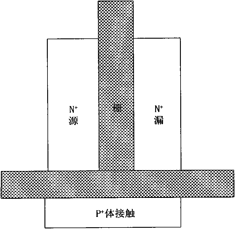
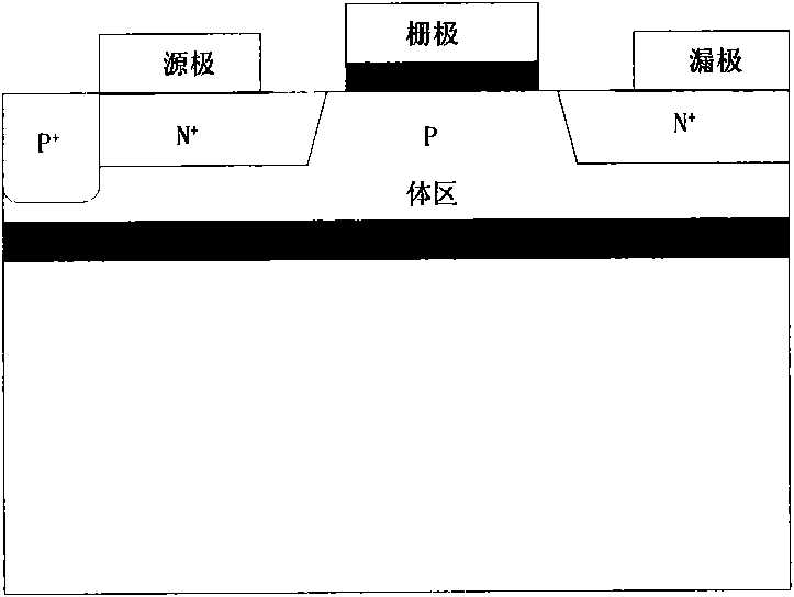
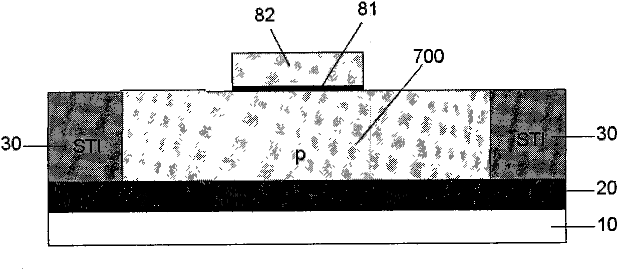
[0021] like Figure 2e As shown, a MOS device structure for suppressing SOI floating body effect includes: a substrate 10, an insulating buried layer 20 on the substrate 10, an active region on the insulating buried layer 20, and the active region on the The upper gate region and the Shallow Trench Isolation (STI) structure 30 around the active region.

[0022] The active region includes: a body region 70, an N-type source region, an N-type drain region 40, and a heavily doped P-type region 60; the N-type source region is composed of a silicide 51 and an N-type Si region 52 connected thereto. The N-type source region and the N-type drain region 40 are located at both ends of the body region 70 respectively; the heavily doped P-type region 60 is located under the N-type Si region 52 of the N-type source region,...


PUM


Abstract

The invention discloses a method for manufacturing an SOI MOS device capable of realizing ohmic contact with a source body, comprising the following steps: firstly manufacturing a grid region; carrying out light dope on a high-dose source region and a high-dose drain region to form a high-concentration light-doped N-shaped source region and a light-doped N-doped drain region; manufacturing a side wall isolation structure around the grid region; carrying out the ion implantation on the source region and the drain region, carrying out heavy-doped P ion implantation obliquely through arranging a mask with an opening in the source region, so as to form a heave-doped P-shaped region between the source region and a body region, and finally forming a layer of metal on of the partial surfaces on the source region; and heating to lead the metal to react with the Si material below the metal to generate silicide. In the method of the invention, the silicide forms ohmic contact with the heavy-doped P-shaped region near the silicide, and releases the holes accumulated by the SOI MOS device in the body region, so as to inhibit the floating body effect of the SOIMOS device, and have the advantages of not increasing the chip area, possessing simple manufacturing process and being compatible with the conventional CMOS process and the like.

Description

technical field [0001] The invention relates to a manufacturing method of a MOS (Metal Oxide Semiconductor) structure, in particular to a manufacturing method of an SOI MOS device which realizes ohmic contact of a source body through a silicide process, and belongs to the technical field of semiconductor manufacturing. Background technique [0002] SOI (Silicon On Insulator) refers to silicon-on-insulator technology. In SOI technology, the device is only fabricated in a very thin silicon film on the surface, and the device and the substrate are separated by a buried oxide layer. It is this structure that makes SOI technology have the incomparable advantages of bulk silicon. Small parasitic capacitance enables SOI devices to have high speed and low power consumption. The full dielectric isolation of SOI CMOS devices completely eliminates the parasitic latch-up effect of bulk silicon CMOS devices, and the full dielectric isolation of SOI makes SOI technology high integration ...

Claims


Application Information

Patent Timeline
IPC IPC(8): H01L21/336H01L21/265H01L29/06
CPCH01L21/28518H01L29/78654H01L29/78612
Inventor 陈静伍青青罗杰馨肖德元王曦
Owner SHANGHAI INST OF MICROSYSTEM & INFORMATION TECH CHINESE ACAD OF SCI
Why Eureka
Try Eureka