

Self-aligned spacer multiple patterning methods
A multi-patterning and spacer technology, which is applied in the photoengraving process, instruments, optomechanical equipment and other directions of the pattern surface, which can solve the problems of cost inefficiency and so on.
- Summary
- Abstract
- Description
- Claims
- Application Information
AI Technical Summary
Problems solved by technology
Method used
Image

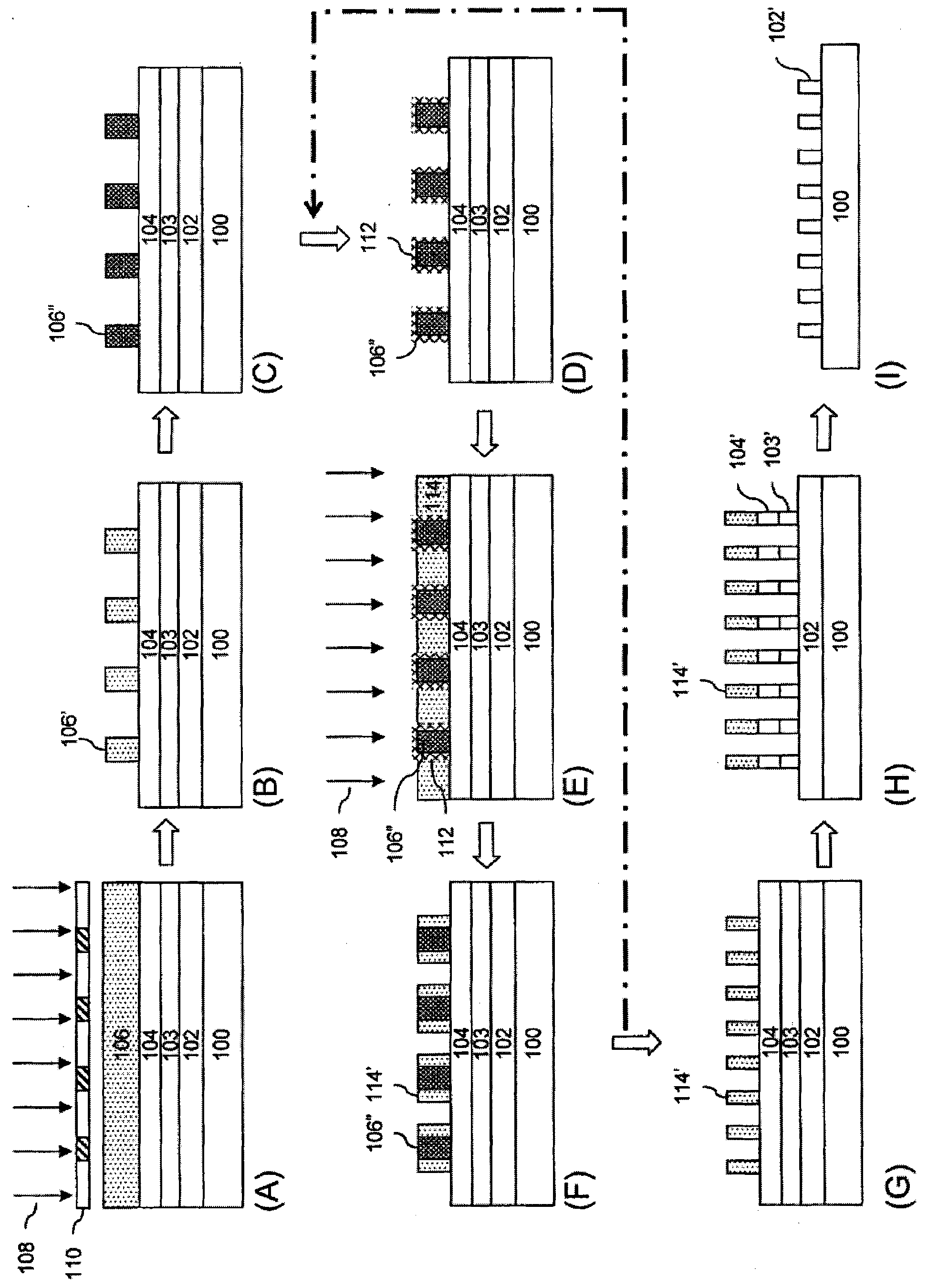
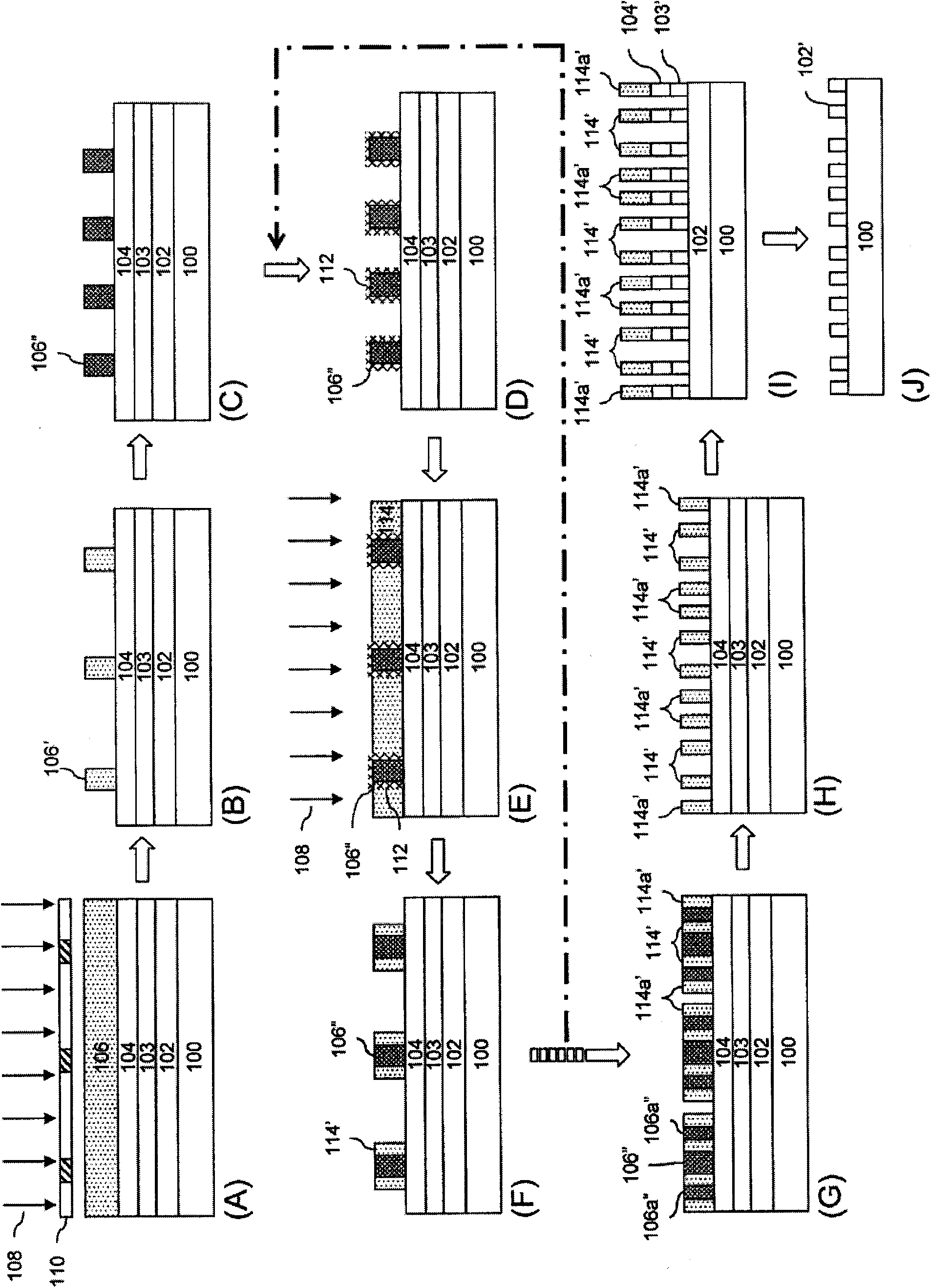
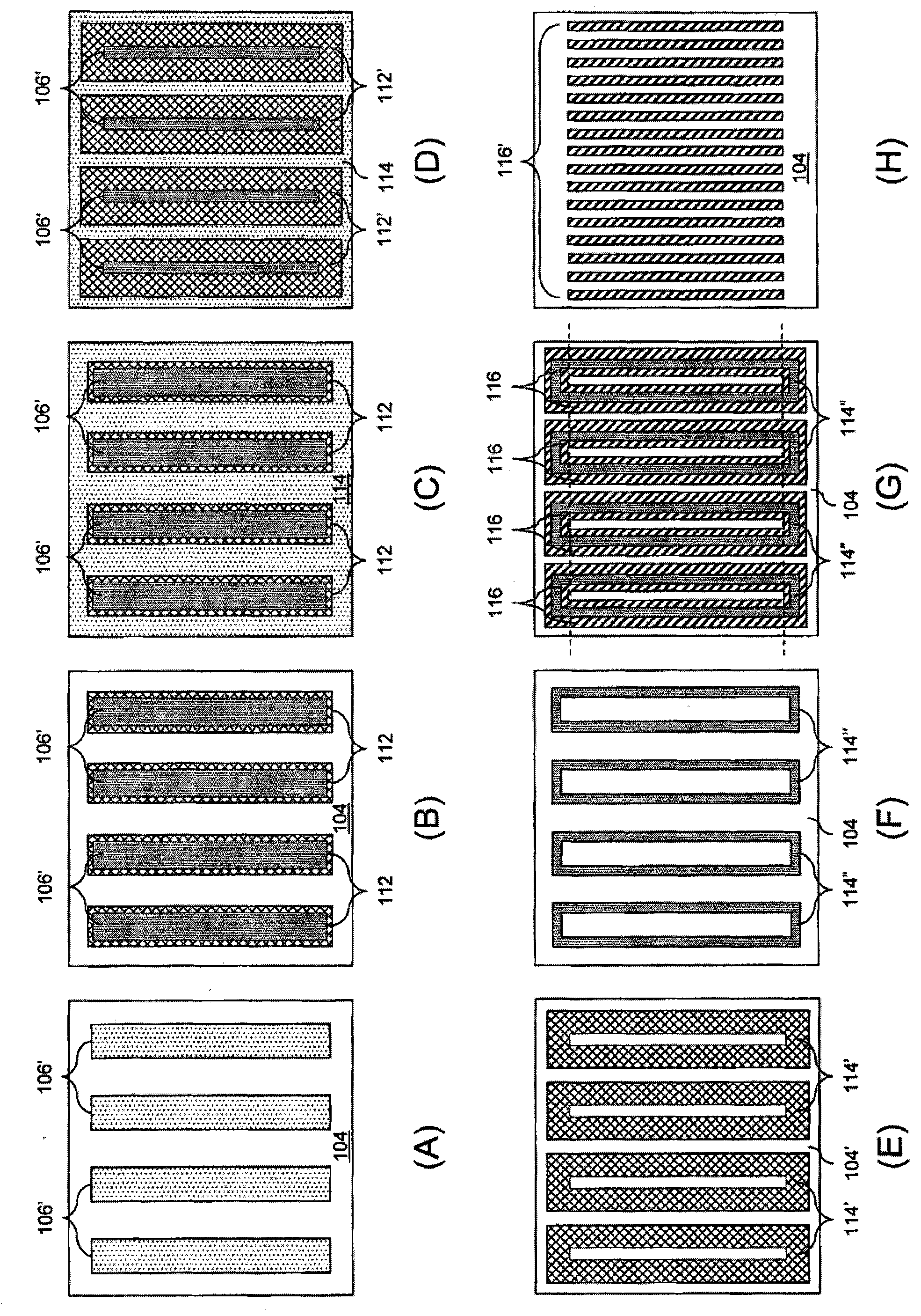
Examples
Embodiment 1
[0073] L1 photoresist polymer (poly(IAM / α-GBLMA / ODOTMA / HAMA)) synthesis
[0074] 10.51 g of 2-methyl-acrylate 1-isopropyl-adamantyl (IAM), 6.82 g of 2-methyl-acrylate 2-oxo-tetrahydro-furan-3yl ester (α-GBLMA), 6.36 g 2-Methyl-acrylic acid 3-oxo-4,10-dioxo-tricyclo[5.2.1.0 2,6 ] Dec-8-yl ester (ODOTMA) and 6.31 g of 3-hydroxy-adamantyl 2-methyl-acrylate (HAMA) were dissolved in 27 g of tetrahydrofuran (THF). The mixture was degassed by bubbling nitrogen gas for 20 min. A 500 ml ampoule equipped with a condenser, nitrogen gas inlet and mechanical stirrer was charged with 11 g of THF and the solution was warmed to a temperature of 67°C. 5.23 g of dimethyl-2,2-azobisisobutyrate (17 mol % based on the whole monomer) were dissolved in 5 g of THF and filled into an ampoule. The monomer solution was flowed into the reactor at a rate of 16.0 milliliters per hour (mL / h) for 3 hours and 30 minutes. The polymerization mixture was stirred for an additional 30 minutes at 67°C. 5 g of ...
Embodiment 2-18
[0088] The above procedure of Reference Example 1 was repeated except that the ingredients listed in Table 1 below were used instead of TAEA and TERGITOL TMN-6 surfactant.
[0089] Table 1
[0090] Example
[0091] It is expected that spacer structures will form after L2 development.
PUM
 Abstract
Description
Claims
Application Information