
Surface plasmon (SPP)-based large-area interference lithography technology

An interference lithography, large-area technology, applied in the field of micro-nano processing

Inactive Publication Date: 2011-02-02
UNIV OF ELECTRONICS SCI & TECH OF CHINA
View PDF0 Cites 15 Cited by
  • Summary
  • Abstract
  • Description
  • Claims
  • Application Information

AI Technical Summary

Problems solved by technology

[0009] The present invention is to overcome the shortcoming that the current SPP interference lithography technology needs a mask, and provides a maskless SPP interference lithography technology to realize super-diffraction resolution nano-pattern processing

Method used


Image

  • Surface plasmon (SPP)-based large-area interference lithography technology
  • Surface plasmon (SPP)-based large-area interference lithography technology
  • Surface plasmon (SPP)-based large-area interference lithography technology

Examples


Embodiment Construction

[0035] specific implementation

[0036] The periodic nanowires produced by the method of the present invention will be described in further detail below in conjunction with the embodiments and with reference to the accompanying drawings:

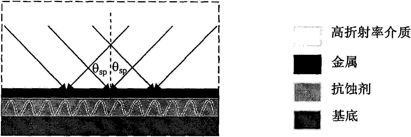
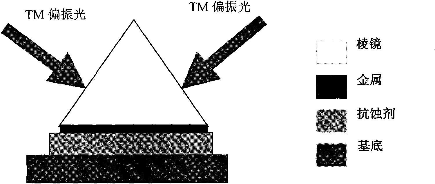
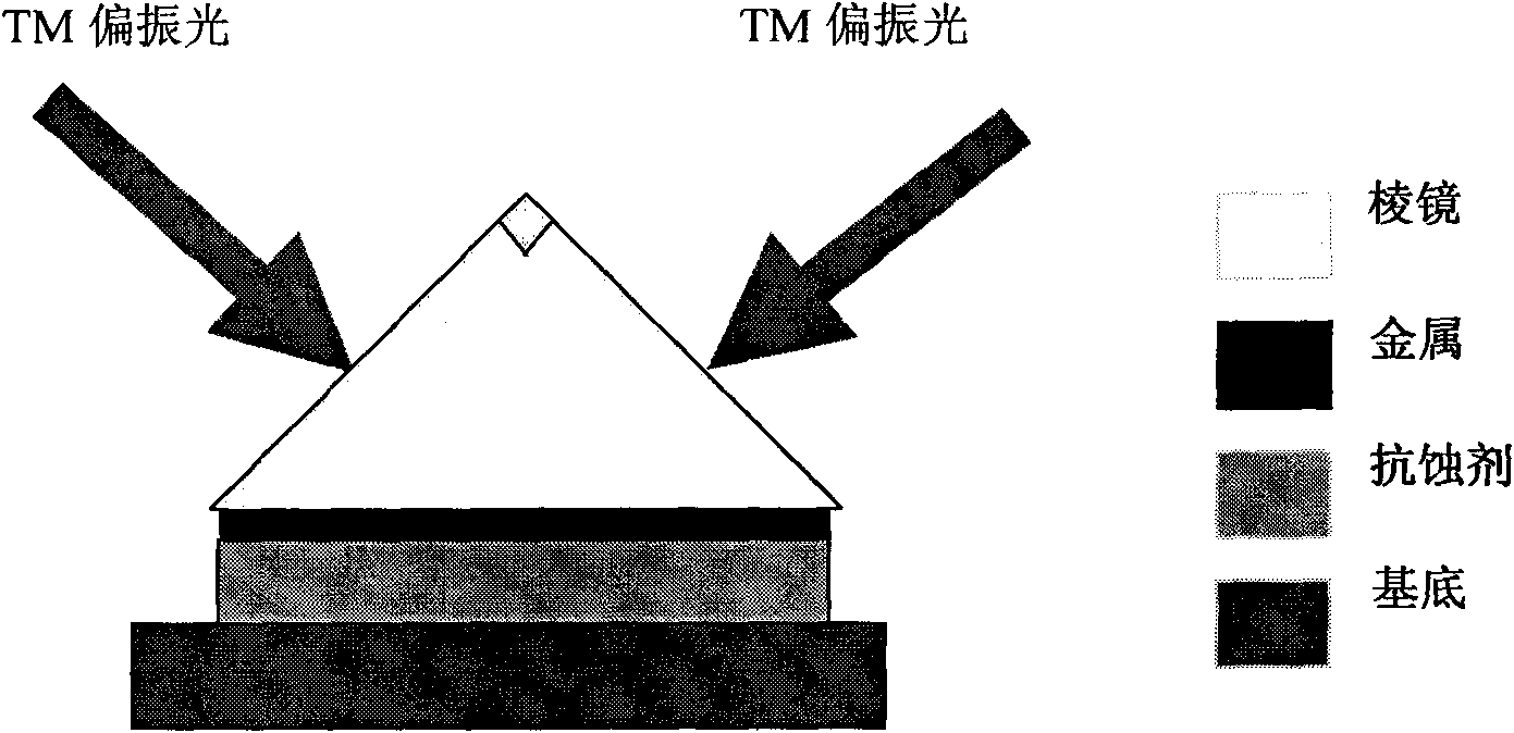
[0037] (1) with Figure 4 For example, make photolithographic dense lines below 65nm.

[0038] Assuming that the incident light source wavelength is 436nm, the refractive index of the equilateral triangular prism is 1.94325 (NLAF36 glass); the metal is silver, and its complex dielectric constant is -8.9170+0.2320i, and the thickness is 40nm; the refractive index of the resist is 1.53 (AZ9200).

[0039] The calculation steps are:

[0040] 1. According to formulas (1) and (2), the resonance angle θ can be calculated sp about 66°;

[0041] 2. According to the formula (4), it can be calculated that the period of the interference fringe Λ = 122nm;

[0042] 3. According to the formula (5), the feature size of the line is R=61nm, which meets ...


PUM


Abstract

The invention provides surface plasmon (SPP)-based large-area interference lithography technology. In the technology, a dielectric layer with high refractive index is irradiated by two broad-beam light sources, the SPP on the surface of metal is excited in an attenuated total internal reflection coupled mode, and mutual interference exists among the SPP, so that a large-area periodic nanometer graph is formed in a resist; the SPP has the function of reinforcing a near field, so the graph has high contrast; meanwhile, the SPP has the characteristic of short wavelength, so high spatial resolution can be obtained and nanowires exceeding diffraction limit can be realized. Compared with the conventional nanometer lithography technology, the technology has the advantages of low lithography cost, large area exposure, no need of a complex and expensive optical imaging system with high numerical aperture, and wide application prospect in the manufacturing of large-scale integrated circuits and novel optical and electronic nanostructure devices.

Description

Technical field [0001] The invention belongs to the field of micro-nano processing, and relates to a photolithographic technology for making high-resolution periodic nanometer patterns. Background technique [0002] At present, nano-device integration and application technology has become the main direction of high-tech development and research in countries all over the world, especially in industrialized countries. Since 2000, the U.S. has invested $6 billion in nanotechnology R&D funds, and the European Union has also invested 1.3 billion euros in the development of nanotechnology from 2002 to 2006. Nanotechnology will become one of the three major technologies that will affect human life in the future. [0003] However, both ultra-large scale integrated circuits and new optical and electronic nanostructure devices require the use of high-resolution, high-efficiency, and low-cost nanoscale processing technologies. As the size of nano-devices continues to shrink and enter...

Claims


Application Information

Patent Timeline
IPC IPC(8): G03F7/20
Inventor 郭小伟刘永智于全福
Owner UNIV OF ELECTRONICS SCI & TECH OF CHINA
Learn More